
Federal Court of Australia
Hanwha Solutions Corporation v REC Solar Pte Ltd [2023] FCA 1017
ORDERS
DATE OF ORDER: |
THE COURT ORDERS THAT:
1. The parties confer and supply to the chambers of Justice Burley by 4pm on 19 September 2023 draft short minutes of order giving effect to these reasons and a proposed timetable for further steps to be taken in the proceedings.
2. Insofar as the parties are unable to agree to the terms of the draft short minutes of order referred to in order 1, the areas of disagreement should be set out in mark-up.
3. The confidential reasons for judgment be published only to those persons who have executed suitable confidentiality agreements as determined in first instance by the solicitors acting for the applicants and the respondents.
4. The non-confidential reasons, which do not include the reasons concerning patent infringement, are published without restriction.
Note: Entry of orders is dealt with in Rule 39.32 of the Federal Court Rules 2011.
CONFIDENTIAL REASONS FOR JUDGMENT
BURLEY J
1.1 The parties and the proceedings
1 These proceedings concern solar cell technology, a claim of patent infringement, a cross claim for the invalidity of the asserted claims of the patent, misleading and deceptive conduct and the making of unjustified threats of patent infringement.
2 Hanwha Solutions Corporation, a company incorporated in South Korea, is the registered proprietor of Australian patent No AU 2008323025, which is entitled “Method for manufacturing a solar cell with a surface-passivating dielectric double layer, and corresponding solar cell”. It and Hanwha Q CELLS Australia Pty Ltd (collectively Hanwha) are the applicants. The patent has a priority date of 14 November 2007.
3 Hanwha initially commenced three sets of proceedings being:
(a) NSD 394 of 2019 against LONGi Green Energy Technology Co Ltd, a company organised under the laws of the Peoples Republic of China, and three other related companies (collectively, LONGi).
(b) NSD 395 of 2019 against Jinko Solar Australia Holdings Co Pty Ltd; and
(c) NSD 458 of 2019, against REC Solar Pte Ltd, a company organised under the laws of Singapore and two other companies that REC Solar has authorised to sell products that Hanwha alleges fall within the scope of the claims of the patents, being Sol Distribution Pty Ltd and Baywa r.e. Solar Systems Pty Ltd. For convenience, I refer to these respondents collectively as REC Solar.
4 As matters transpired, after the hearing, but before judgment, the proceedings in (a) and (b) settled. As I explain in section 1.5 below, each of LONGi, Jinko and REC Solar co-operated in the conduct of the proceedings so that there was no unnecessary duplication in their approach to the invalidity case. The consequence was that, leaving aside the separate allegations of infringement against LONGi and Jinko, the content of the matters in controversy remained largely unchanged as a result of the settlements.
1.2 The case asserted by Hanwha
5 In its seventh amended statement of claim, Hanwha alleges that multiple products sold and offered for sale by or with the approval of REC Solar (REC Solar products) fall within the scope of asserted claims 12, 13, 14, 16, 17, 18, 19 and 21 of the patent. Hanwha also alleges that by reason of its infringing conduct REC Solar has falsely represented that one or more of the accused REC Solar products do not infringe any intellectual property rights and that it is legally entitled to sell and third parties are entitled to purchase, install and use those products in breach of the Australian Consumer Law being schedule 2 to the Competition and Consumer Act 2010 (Cth) (ACL claim).
6 REC Solar denies that the REC Solar products fall within the scope of the asserted claims and also advances a cross claim alleging that those claims are not valid.
1.3 The responsive case advanced by REC Solar
7 In its fourth amended particulars of invalidity REC Solar relies on lack of novelty, lack of inventive step, lack of fair basis, inutility and lack of clarity as grounds. It also contends that Hanwha made unjustified threats of patent infringement, in breach of s 128 of the Patents Act 1990 (Cth). I note that the version of the Patents Act applicable to the proceedings is that following the amendments made by the Patents Amendment Act 2000 (Cth) but before those made by the Intellectual Property Laws Amendment (Raising the Bar) Act 2012 (Cth) (RTB Act).
8 In its Amended Consolidated Particulars of Invalidity (POI), REC Solar sets out the grounds upon which it contends that claims 9, 11-14 and 16-21 (challenged claims) ought to be revoked.
9 In its novelty challenge as advanced in its closing submissions, REC Solar contends that, by reason of the publication of the documents identified below, the claims identified are not novel in accordance with s 18(1)(b)(i) of the Act (grounds 1, 2 and 3):
(a) International Patent Application WO 2008/065918 A1 entitled “Solar cell and method of manufacturing the same” (Isaka) is said to invalidate claims 9, 11-14, 17-19 and 21 of the patent;
(b) US patent application 2006/0102972 A1 entitled “Optoelectronic devices, solar cells, method of making optoelectronic devices, and methods of making solar cells” (Bhattacharyya), published 18 May 2006, is said to invalidate claims 9 and 11 of the patent; and
(c) US patent 4,463,216 entitled “Solar Cell” (Nakano), published 31 July 1984, is said to invalidate claims 9, 12, 16 and 21 of the patent.
10 In its lack of inventive step challenge, REC Solar contends that the invention in the challenged claims is not patentable for want of an inventive step within the meaning of s 18(1)(b)(ii) of the Act by reason that a person skilled in the art in light of the common general knowledge before 14 November 2007 together with the following documents considered separately or together (ground 4):
(a) An article entitled “Ultralow surface recombination of c-Si substrates passivated by plasma-assisted atomic layer deposited Al2O3” by B. Hoex et al (Hoex 2006); and
(b) An article entitled “Excellent passivation of highly doped p-type Si surfaces by the negative-charge-dielectric Al2O3” by B. Hoex et al (Hoex 2007)
would find the invention to be obvious.
11 In relation to its challenge on the basis of lack of fair basis, REC Solar advances six contentions.
12 First, it contends that the challenged claims travel beyond the matter described in the specification in that there is no real and reasonably clear disclosure in the specification of a solar cell, or a method for manufacturing such a solar cell, having a first dielectric layer formed by means other than atomic layer deposition (ALD) (ground 5).
13 Secondly, it contends that if claim 9 is construed such that the “silicon substrate” may have a silicon oxide layer on its surface, then the specification does not comply with s 40(3) of the Act in that claim 9 and claims 11-14 and 16-21 when dependent on claim 9 are not fairly based on the specification (ground 6).
14 Thirdly, it contends that if the challenged claims encompass a solar cell or method of making such a cell with material other than aluminium oxide on a surface of the silicon substrate, those claims travel beyond the matter described in the specification (ground 7).
15 Fourthly, if claim 9 is construed such that it encompasses a solar cell which is not manufactured by a method which includes depositing a first dielectric layer comprising aluminium oxide on a surface of the silicon substrate, then claim 9 and claims 11-14 and 16-21 when dependent on claim 9 travel beyond the matter described in the specification (ground 8).
16 Fifthly, each of claims 9, 11-14, 16 and 21 travel beyond the matter described in the specification in that:
(a) Insofar as it includes a silicon substrate having a lightly doped region of conduction type n it includes a solar cell or a method of manufacturing a solar cell in which an inversion layer is induced below the passivating layer, and in which a parasitic shunt may form; and
(b) There is no real and reasonably clear disclosure of such a solar cell or method of manufacturing such a cell.
(ground 9)
17 Sixthly, each of the challenged claims travels beyond the matter described in the specification as the specification discloses a second dielectric layer with a high hydrogen content (of at least 1 atomic percent (at. %) preferably at least 2 at. % and more preferably at least 5 at. %) and each of those claims are not so limited (ground 10).
18 In ground 12, REC Solar contends that the alleged invention as claimed in the challenged claims is not a patentable invention for the purposes of s 18(1)(c) of the Patents Act for lack of utility in that those claims include solar cells containing dielectric layers that do not achieve the promise of the invention.
19 REC Solar contends that the specification of the patent does not comply with the requirements of s 40(3) of the Patents Act in that claims 16, and claims 17-21 to the extent that they are dependent on claim 16, are not clear and succinct because:
(a) In ground 20, the phrase “wherein the surface of the silicon substrate is passivated by hydrogen” is unclear and ambiguous and there is no workable standard for determining whether that feature is present;
(b) In ground 20A, if the phrase “hydrogen being embedded into the second dielectric layer” in claim 9 is construed so as to require a minimum concentration of hydrogen, then it is ambiguous because there is no workable standard for determining whether the feature is present.
20 For completeness, I note that grounds 11 and 13-19 of the POI were not pressed by REC Solar in closing submissions.
21 For the reasons set out in this judgment I have found that the REC Solar products do not fall within the scope of claim 9 of the patent, and accordingly none of the asserted claims are infringed because each of the asserted claims is dependent upon claim 9. As a result, the ACL claim advanced by Hanwha, which depended on a finding of infringement, also fails. The unjustified threats claim advanced by REC Solar succeeds.
22 I also find that claims 9, 12, 16 and 21 are invalid for want of novelty in the light of Nakano but that otherwise the invalidity challenges advanced by REC Solar fail.
23 REC Solar has asserted confidentiality over much of the information concerning the make-up of the REC Solar products. Accordingly, I will not publish the infringement section of these reasons until the parties have had an opportunity to consider whether an agreed (redacted) version of that section can be released. The only orders that I will make are for the parties to confer and supply to my chambers within 21 days draft short minutes of order giving effect to these reasons, and a proposed timetable for further steps to be taken in the proceedings.
1.5 Relevant aspects of case management of the three proceedings
24 The proceedings were complicated and hard-fought. Prior to the settlements reached between Hanwha, LONGi and Jinko, the management of the case involved dealing with three sets of allegations of infringement concerning multiple products manufactured by each of the three sets of respondents. All parties are fierce competitors in the emerging field of solar cell production. Each maintained a high degree of confidentiality in their products and processes of manufacture.
25 The conduct of the proceedings is a testament to the good sense of the parties and the professionalism of their advisors. In all three of the cases, the parties consented to (or did not inordinately oppose) a number of significant case management steps that enabled the proceedings to be managed together and conducted efficiently.
26 The following aspects of the management of the case warrant mention:
(1) Early in the proceedings the respondents accepted that they should be permitted one substantive witness to give evidence going to questions of invalidity. This considerably eased the progress of the trial and eliminated unnecessary duplication. The invalidity expert retained by the respondents was Professor Weber, to whom I refer below.
(2) Before the preparation of evidence in chief, REC Solar, LONGi and Jinko each filed and served a Product Description of the products alleged to be infringed and a position statement of non-infringement concerning each of the impugned products. Hanwha responded with a position statement on infringement that identified any factual or legal matters in dispute arising from the respondents’ position statement.
(3) A technical primer was prepared using a process whereby, when Hanwha served its expert affidavit evidence in chief on infringement, it identified a portion that included what was intended to be an uncontroversial introduction to the relevant technology and a glossary of relevant terms at the priority date. In their expert affidavit evidence in chief on validity, the respondents identified what was also intended to be an uncontroversial portion of that affidavit that included a summary of the relevant common general knowledge to the skilled addressee before the priority date. Each side’s expert responded to these sections and then the parties jointly served and filed the primer and statement of common general knowledge, which included a mark-up indicating any areas of disagreement between them.
(4) Although each of the respondents pleaded separate particulars of invalidity, shortly before the trial they cooperated to produce one consolidated set of particulars of invalidity, thereby limiting unnecessary repetition.
(5) The parties agreed to suitable confidentiality regimes during the preparation of the proceedings to ensure that, whilst their confidential manufacturing processes were protected, sufficient disclosure was provided to the other parties to enable the legal advisors to understand how the case would run. This involved a complicated regime with multiple levels of confidentiality that required ongoing cooperation between the parties and minimal involvement by the Court.
(6) Orders were made that all issues of liability, including as to infringement, contravention of the ACL and unjustified threats under s 128 of the Patents Act, were to be determined separately and before any issues of election and quantification of pecuniary relief (including any additional damages).
(7) The respondents had divergent interests on the question of infringement. Whilst they relied on the evidence of Professor Weber in support of their grounds of invalidity, each relied upon the evidence of separate experts in support of the non-infringement defences (being Dr Glew (REC Solar), Dr Ruby (Jinko) and Professor Weber (LONGi)).
(8) Those experts who were involved in giving evidence concerning infringement issues, but who were not involved in giving evidence concerning the validity of the patent, were not invited to participate in the preparation of joint expert reports concerning validity, or the subsequent concurrent evidence sessions addressing that topic.
(9) The experts, with the assistance of a Judicial Registrar of the Court, participated in meetings prior to the hearing and produced six separate joint expert reports (JER), three concerning infringement issues (REC Solar, Jinko and LONGi JER respectively), one concerning claim construction (Construction JER) and two concerning invalidity issues (Validity JER).
(10) The oral and written evidence of the experts in all three proceedings given by Professor Weber, Dr Glew, Dr Ruby, Dr Rentsch, Professor Cuevas-Fernandez and Dr Winderbaum, including the JER, was taken as evidence in all of the proceedings.
(11) One issue arose during the course of objections to evidence, when Hanwha expressed concern that the infringement experts, in giving evidence going to construction, might be considered also to have given expert evidence relevant to the questions of fair basis and inutility of the patent. Those concerns did not arise out of any improper instructions to the experts, but rather because, naturally enough, it was necessary for each expert to construe the claims in the context of the specification as a whole, which led them to express views as to the breadth of the claims in the context of the invention disclosed as a whole. To ensure that the experts maintained the roles envisaged for them early in the proceedings, and bearing in mind that Professor Weber had separately given evidence concerning all invalidity issues, particular paragraphs identified by Hanwha were made the subject to a limitation under s 136 of the Evidence Act 1995 (Cth) to the effect that those paragraphs may not be relied upon for the purposes of the fair basis or utility challenges (as the case may be) to the validity of the patent.
2.1 Hanwha – the REC Solar U Cell
27 Magnus Garbrecht is a Senior Transmission Electron Microscopy (TEM) Manager at Sydney Microscopy & Microanalysis at the University of Sydney, specialising in aberration-corrected high-resolution TEM imaging and spectroscopy techniques in the field of materials science. He has a Diploma in Physics and a PhD in Materials Science from the Institute for Experimental and Applied Physics, Christian-Albrechts-University in Kiel, Germany. Dr Garbrecht gives evidence about TEM analysis he and Ms Pillai (see below) undertook on a sample of the REC Solar product identified as the U Cell. He was not cross-examined.
28 Ashalatha Indiradevi Kamalasanan Pillai is a Scanning Electron Microscopy (SEM) Specialist at Sydney Microscopy & Microanalysis at the University of Sydney. In this role, she provides technical support in SEM and Focused Ion Beam (FIB) techniques. Ms Pillai gives evidence about TEM analysis she and Dr Garbrecht undertook on a sample of the U Cell that was prepared by the use of a FIB. She was not cross-examined.
29 Mohanad Mursi is a Manager at the Centre for Advanced Structural Engineering in the School of Civil Engineering at the University of Sydney. He holds a PhD in Civil Engineering and a second PhD in Structural Engineering from the University of New South Wales. Dr Mursi gives evidence about work undertaken by himself and his colleagues at the Centre for Advanced Structural Engineering in relation to extracting samples of U Cells from the U solar modules for subsequent testing. He was not cross-examined.
30 Udit Sharma is a scientific fellow at Eurofins EAG Materials Science. In this role, he facilitates, manages, oversees and reports upon the testing and analysis of a range of industrial materials including in the field of solar cell technology. Mr Sharma gives evidence regarding testing undertaken by EAG of the Sing, Vina, MS, MMS and MV Cells. Mr Sharma was not cross-examined.
31 Jae Sung Lee, is an R&D researcher employed by REC Solar in the Cell R&D Department. In this role he is responsible for researching and developing new technology, including in the field of solar cells, and testing and analysing solar cells, including engaging external service providers to undertake testing and analysis of REC Solar products. Mr Lee gives evidence regarding testing undertaken by WinTech Nano-Technology Services Pte Ltd of the NSP and Solartec Cells. He was not cross-examined.
32 Shankar Gauri Sridhara is the Chief Technology Officer employed by REC Solar. Prior to this position, he joined the REC Scan Module AB division of REC in Sweden, joined the Singapore division of REC as a director of module technology in 2011, and assumed responsibility for the entirety of research and development in REC from poly-silicon to products in 2016. Dr Sridhara was responsible for preparing:
(1) REC Solar’s product description (REC-PD), which involves his interpretation of testing undertaken by WinTech of the Sing, Vina, NSP and Solartec Cells; and
(2) REC Solar’s second supplementary product description (REC-SSPD), which involves his interpretation of testing undertaken by WinTech of the MS and MMS Cells and his interpretation of testing undertaken by EAG of the MV Cell.
33 Dr Sridhara verifies the REC-PD and REC-SSPD relied upon by REC Solar in these proceedings, and gives evidence providing the primary sources and contemporaneous documents referred to and relied upon in the REC-PD and REC-SSPD. Dr Sridhara was cross-examined.
34 John Lee is a partner at Gilbert + Tobin, the solicitors acting for REC Solar. He gives evidence annexing correspondence relevant to REC Solar’s unjustified threats cross-claim. He was not cross-examined.
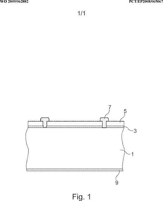
35 Jochen Rentsch is Department Head, PV Production Technologies – Surfaces and Interfaces, at the Fraunhofer Institute for Solar Energy Systems in Freiburg, Germany. He has previously provided expert evidence in relation to patent infringement proceedings in Germany between companies related to Hanwha on the one hand and companies related to the respondents on the other concerning a European patent No 2 220 689, which is related to the patent. In 2002 Dr Rentsch completed a degree in physics whereupon he began a PhD thesis entitled “Dry production technologies for crystalline silicon solar cells” at Albert-Ludwigs University in Frieburg. In 2005 he commenced working for his current employer focussing on research in solar cell and photovoltaics production technologies and in particular upon deposition and etching processes and technologies.
36 Dr Rentsch has given six affidavits in these proceedings which address questions of infringement and validity of the patent (excluding lack of inventive step). He participated in the preparation of the Construction JER and infringement JERs for each of the LONGi, Jinko and REC Solar infringement cases and the matching concurrent evidence sessions for each.
37 Andres Cuevas-Fernandez is an Emeritus Professor at the Australian National University (ANU). He has worked in the field of silicon solar cell technology since 1976. He received an undergraduate degree in telecommunications engineering at the Universidad Politecnica de Madrid in 1976 and conducted research in the area of silicon solar cells in the Laboratorio de Semiconductores to earn his PhD from the same university in 1980. He has since worked in various teaching and research positions. In July 1993 he moved to the ANU where he was the head of the School of Engineering from 2007 until 2010. He retired in April 2018 whereupon he took an appointment as Emeritus Professor.
38 In his affidavit Professor Cuevas-Fernandez describes himself as one of the most experienced researchers in the field of photovoltaics, having contributed to the scientific and technological advancement of silicon solar cells since 1976. He has collaborated extensively with many of the leading researchers and research institutes in the field and also with workers in industrial settings. He is a named inventor on 12 patents and patent applications. His research has almost entirely been devoted to wafer-based silicon solar cell technology.
39 Professor Cuevas-Fernandez gave one affidavit addressing the validity of the patent and participated in joint expert reports and concurrent evidence sessions concerning the alleged lack of inventive step in the patent.
40 Professor Cuevas-Fernandez participated in the preparation of the two Validity JERs concerning the obviousness case and the matching concurrent evidence sessions for each.
41 Saul Winderbaum is a retired adjunct associate professor at the University of New South Wales and Director of Shamash Australia Pty Ltd. From 1984 until 1993 he worked as a process engineer in the production of microelectronic components. In 1998 he was awarded a PhD for a thesis entitled “Optical enhancements in silicon solar cells” by the University of New South Wales. Prior to commencing work on his PhD thesis, Dr Winderbaum had used Plasma-Enhanced Chemical Vapour Deposition (PECVD) extensively in microelectronics to deposit silicon nitride layers. He developed this use of PECVD in depositing silicon nitride on silicon wafers in the context of solar cells in his PhD research. In 2000 he took a position as senior scientist at BP Solar where he was responsible for modifying their manufacturing processes to establish the use of silicon nitride deposited by PECVD as an anti-reflective coating. In 2003 Dr Winderbaum became a consultant to BP and other companies in the solar cell industry.
42 Dr Winderbaum participated in the preparation of one Validity JER relating to the question of inventive step and the equivalent concurrent evidence session.
43 Klaus Weber is a Professor in the School of Engineering at the ANU. He was awarded a Bachelor of Electrical Engineering from the University of Adelaide in 1992 and a PhD in Engineering for a thesis entitled “Liquid phase epitaxy of silicon for thin film silicon solar cells” from the ANU in 1997. His research focussed on producing silicon films of 0.01 to 0.08 mm thickness to evaluate and demonstrate the potential of such films for use in low cost, high efficiency silicon solar cells.
44 From 1998 until 2014 he conducted research at the ANU. During his time as a post-doctoral fellow at ANU, he worked in collaboration with Boral Energy (later called Origin Energy) on a technique that he had assisted in developing (called “epilift”) to detach thin silicon films from the substrate on which they were formed. He continued this research from 1998 until 2001, which included trying to scale it up for industrial use. Also in collaboration with Origin Energy, from 2000 to 2001 Professor Weber assisted in the development of a new technology for the fabrication of thin silicon solar cells which became the subject of several patents. From 2002 to 2014 Professor Weber continued to work on developing this technology. From 2001 to 2007 Professor Weber was also involved in researching various properties of low pressure chemical vapour deposition (LPCVD) silicon nitride for use in solar cells.
45 Professor Weber has published over 140 papers and is a named inventor on 14 patents or patent applications, most of which pre-date the priority date. In his oral evidence he accepted that he was a leading figure in solar cell research who was doing original, cutting-edge research and who, when pressed, accepted that he was “moderately inventive”.
46 Professor Weber gave evidence relevant to the validity of the patent and the question of infringement in relation to the alleged infringement by the LONGi products. He participated in the preparation of the Construction JER, the LONGi infringement JER and the Validity JER and he gave concurrent evidence in sessions concerning these topics.
47 Alexander David Glew is a materials scientist and mechanical engineer. His academic credentials include a Bachelor of Science and a Masters of Science in Mechanical Engineering from the University of California, Berkeley received respectively in 1985 and 1987, a Master of Science in Materials Science and Engineering from Stanford University in 1995 and a PhD in Materials Science and Engineering from Stanford University in 2003. The subject of his doctoral dissertation related to PECVD of dielectric films.
48 Dr Glew worked from 1987 until 1997 for Applied Materials Inc, a company that manufactures the equipment used to make semiconductors and sells that equipment to companies who make semiconductors. He had various roles within the company, with particular emphasis on chemical vapour deposition, a process involving the mixing of two or more gasses in a process reactor or chamber and having them meet on the surface of a substrate to deposit a thin film which, in the semiconductor or solar industry, would be 2 to 3 nanometres (nm) or less. In 1997 he left Applied Materials and became the president of his own company, Glew Engineering, which provides consulting services to various technology or engineering areas, including chemical vapour deposition technology. He has assisted component suppliers and equipment suppliers on various projects including in relation to gas panel design, integrated circuits failures and semiconductor equipment failures. His company’s practice includes multi-physics finite element analysis.
49 In his first affidavits, Dr Glew was provided a review of the patent and was asked to consider whether the REC Solar Multi Sing, Multi Vina, NSP and Solartec Cells fall within claims 9, 11-14 and 16-21 of the patent and to respond to the evidence of Dr Rentsch. In his second affidavit he was asked to consider whether three additional solar cells, referred to as the MS, MMS and MV cells infringed those claims and respond to further evidence from Dr Rentsch. In his third affidavit, Dr Glew was asked to consider whether the U Cell fell within the claims and to respond to further evidence from Dr Rentsch. In his fourth affidavit, Dr Glew was provided with certain documents annexed to the affidavit of Mr Lee concerning testing performed by WinTech on the Solartec and NSP products.
50 Dr Glew participated in the preparation of the Construction JER and the REC Solar infringement JER.
51 Douglas Scott Ruby is a consultant in the photovoltaics industry. He studied physics in university and was awarded a Bachelor of Science from the Massachusetts Institute of Technology in 1978 and was awarded a Masters and PhD from the University of Illinois specialising in semiconductor physics in 1980 and 1985 respectively. After his PhD, he worked for Sandia National Laboratories as a researcher from 1985 until 2008 working in its photovoltaics solar cell research division where he focussed on devising methods and procedures which could be employed in solar cell manufacturing to make solar cells more efficient or less expensive to manufacture. In about 1999, Dr Ruby became the leader of his division’s photovoltaic cell development team, managing seven researchers including in work directed towards improving surface passivation and reducing surface reflectance.
52 In his first affidavit Dr Ruby gave his views as to the disclosure of the patent and the construction of the claims and expressed views concerning the alleged infringement of certain claims by the Jinko products (which are not relevant to the present proceedings). In his second affidavit he provided some clarification of a point made in his first affidavit.
53 Dr Ruby was involved in the preparation of the Construction JER and the Jinko infringement JER and gave concurrent evidence in sessions concerning those topics.
4. THE AGREED COMMON GENERAL KNOWLEDGE
54 Annexure A to this judgment consists of parts of the primer and agreed common general knowledge document provided by the parties. It was prepared as a result of an iterative process. It arises from a combination of the evidence of Dr Rentsch and Professor Weber insofar as it provides an explanation of some relevant background concepts, and a combination of evidence of Professor Weber and Professor Cuevas-Fernandez insofar as it concerns matters going to common general knowledge relevant to the question of whether or not the invention claimed involves an inventive step. It has been edited to address more central aspects of the technology. To the extent that the parties did not agree on its content, Annexure A includes my findings as to the common general knowledge. It is recommended reading for those not familiar with the technology in the patent.
55 The patent relates to the production of a more efficient solar cell using a double dielectric layer stack that reduces recombination losses by increasing surface passivation. The specification is to be understood in the light of the common general knowledge of the persons skilled in the art, including the information set out in Annexure A.
56 The patent is entitled “Method for manufacturing a solar cell with a surface-passivating dielectric double layer, and corresponding solar cell” and the field of the invention is described in the same terms.
57 The Background of the Invention first provides a reference to the technology (page 1 line 20):
A key requirement for achieving high degrees of efficiency in solar cells is very effective suppression of surface recombination losses. For this purpose, the surface of solar cells should be passivated as effectively as possible, so that charge carrier pairs which are generated inside the solar cell by incident light and which diffuse to the surfaces of the solar cell substrate do not recombine at the solar cell surface, so that they would no longer be available to help improve the efficiency of the solar cell.
58 The Background then identifies four relevant approaches to the problem present in the prior art and difficulties said to arise from that art.
59 The first approach, which is said to arise in laboratory solar cells but not to be in general use in the industrial manufacture of solar cells, is the growing of silicon dioxide at a high temperature (greater than 900 °C). However, this not only adds expenditure in solar cell processing but also has a further difficulty in that high temperature oxidation can lead the more economical multicrystalline silicon to experience “a considerable reduction in material quality” in that the charge carrier lifetime is reduced and thus the wafter has losses in efficiency.
60 The second approach is referred to as a low-temperature alternative, which is surface passivation using amorphous silicon nitride or silicon carbide which can be prepared at temperatures of 300-400 °C by PECVD. The specification provides references to two publications, one by T. Lauinger et al, and another by I. Martin et al. It says that the dielectric layers produced in this way can be used only to a limited degree for large-area, high efficiency solar cells because they contain a high density of “pinholes”, being small holes or pores in the layer, so that they may not have good insulating properties. A further problem with this approach is said to be that (page 2 line 18):
… their passivating effect is based largely on a very high positive charge density within the dielectric layers that can lead, during the passivation of the back of the solar cell if a p-type silicon wafers are used, for example, to the formation of an inversion layer via which an additional leakage current of minority charge carriers can flow away from the base of the solar cell to the back contacts (what is known as a “parasitic shunt”). On highly doped p+ silicon surfaces, silicon nitride can even lead, on account of the high positive charge density, to depassivation compared to an unpassivated p+ surface.
61 The third approach is using amorphous silicon layers which can also be produced by PECVD at very low coating temperatures of typically greater than 250 °C. While very good surface passivation was achieved (page 3 lines 7-14):
… the surface-passivating property of amorphous silicon layers of this type may be very susceptible to temperature treatments. In current-day industrial solar cell processes, the metal coating is in many cases carried out by means of screen printing technology, the last process step typically being a firing of the contacts in a continuous infrared furnace at temperatures of between approx. 800 °C and 900 °C. Although the solar cell is exposed to these high temperatures only for a few seconds, this firing step can lead to considerable degradation of the passivating effect of the amorphous silicon layers.
62 The fourth approach is using aluminium oxide layers which are deposited by means of ALD at about 200 °C, for example, and then tempered at about 425 °C. Using this approach, whilst good passivating results are said to have been achieved, only a single molecular layer is generally deposited on the substrate surface within each deposition cycle.
63 As a deposition cycle typically lasts about 0.5 to 4 seconds (s), correspondingly low deposition rates are obtained. The deposition of aluminium oxide layers at a thickness which is suitable for use as an antireflection layer or as a back reflector therefore requires deposition durations which have in the past shown a use of such layers in industrially produced solar cells to be commercially disadvantageous.
64 The Summary of the Invention then observes that there may be a need for a solar cell and a method for manufacturing in which on the one hand, good passivation of the surface of the solar cell can be achieved and, on the other hand (page 4 lines 1-3):
… the above-mentioned drawbacks of conventional surface-passivating layers can be at least partially avoided. In particular, it should be possible to produce solar cells displaying very good surface passivation in an economical, industrially viable manner.
65 The specification describes a first aspect of the invention (page 4 line 6 to page 5 line 18):
According to a first aspect of the present invention, a method is proposed for manufacturing a silicon solar cell, including the following steps: providing a silicon substrate; depositing a first dielectric layer on a surface of the silicon substrate by means of atomic layer deposition, wherein the first dielectric layer comprises aluminium oxide; and depositing a second dielectric layer on a surface of the first dielectric layer, the materials of the first and the second dielectric layer differing and hydrogen being embedded into the second dielectric layer.
This first aspect of the present invention may be regarded as being based on the following idea: a method is specified for manufacturing silicon solar cells with a dielectric passivating layer for reducing surface recombination losses. The dielectric passivating layer is composed of two partial layers, of a very thin aluminium oxide-containing layer, which is formed by atomic layer deposition (ALD), and also of a thicker layer made of silicon oxide, silicon nitride or silicon carbide, for example, which can be deposited on the aluminium oxide layer by means of plasma enhanced chemical vapour deposition (PECVD), for example.
The dielectric double layer produced in the method according to the first aspect allows the passivation of both high and low-doped regions of the solar cell surface of conduction type p or n. It is possible to allow stable passivation which retains its passivating properties even after a firing step in the temperature range of 800-900 °C for burning-in of metal contacts. At the same time, the dielectric passivating layer can also have advantageous optical properties, i.e for application to the front of the solar cell, the layer can serve as an effective antireflection layer; during application to the back of the solar cell, the passivating layer can form, together with metal coating over the entire area of the back, an effective mirror for photons with energies close to the silicon band gap in order to improve what is known as “light trapping”, i.e. the trapping of light by multiple internal reflection, in the solar cell. Furthermore, the negative effect of “parasitic shunting”, which is known from silicon nitride, can be avoided for rear surface passivation on standard solar cell semiconductor material of conduction type p.
66 In a passage much emphasised by the parties, the specification continues (page 5 lines 10-16):
The key to understanding the outstanding passivating effect and tempering stability of the stack layer according to the invention may be identified in the combination of the Si/Al2O3 interface, which is ideally atomically flat and is produced as a matter of course during the ALD process, and the highly hydrogenous SiOx, SiNx or SiCx layers, such as are formed during the PECVD process, for example. A part of the hydrogen from the PECVD-deposited layers can diffuse through the ultrathin Al2O3 layer and passivate unsaturated silicon bonds at the interface to the silicon.
(Emphasis added)
67 The reference above to the “Si/Al2O3 interface” is to the point of interaction between the previously described silicon wafer and the very thin aluminium oxide layer.
68 The specification then continues by describing features, details and possible advantages of embodiments of the manufacturing method. This commences by noting that the silicon substrate “may be a thin monocrystalline or multicrystalline silicon wafer or else a silicon thin wafer”. The specification notes that the front of the solar cell substrate that faces the incident light (sun) may be coated, in which case the second dielectric layer is applied preferably as an antireflection layer, which is at a thickness at which negative interferences occur for the incident and reflected light. This may be from about 50 to 150 nm in thickness. Alternatively, the back may be coated, in which case the second dielectric layer is embodied as a “back surface reflector” so that light which penetrates the entire solar cell is for the most part reflected at that surface and thus passes through the solar cell substrate a further time.
69 In a further passage that gave rise to considerable debate in submissions, the specification describes that the first dielectric layer may be applied by reference to three steps, first a cleaning of the silicon substrate (page 6 lines 6-12):
Before the depositing of the first dielectric layer, the surface of the silicon substrate can be thoroughly cleaned, so that no contamination remains thereon that might disturb the subsequently deposited dielectric layer. In particular, the surface of the silicon substrate can be slightly etched away, for example in a solution which on the one hand contains an oxidising agent and which on the other hand contains hydrofluoric acid (HF) which etches away the oxidised silicon oxide. A suitable cleaning method known in the production of solar cells is for example what is known as RCA cleaning.
70 The next step in one embodiment is the application of the aluminium containing layer (page 6 line 15 to page 7 line 4):
According to one embodiment of the method according to the invention, for the atomic layer deposition of the first dielectric layer, the silicon substrate is firstly flushed with an aluminium-containing compound comprising at least one of the components Al(CH3)3, AlCl3, Al(CH3)2Cl and (CH3)2(C2H5)N:AlH3, so that an aluminium-containing layer is deposited on the surface of the silicon substrate. Subsequently, the aluminium-containing layer is oxidised to higher valency in an oxygen-containing atmosphere.
During the flushing of the silicon substrate with the aluminium-containing compound, the aluminium-containing compound can cling to the silicon surface at the points at which it enters into contact with the silicon surface. A chemical reaction with the silicon surface can occur; this is also referred to as chemisorption. In the best of cases, this can lead to the formation of a monomolecular layer made up of molecules of the aluminium-containing compound. It may be advantageous in this regard that this molecular layer can be almost perfectly tight, i.e. on correct selection of the processing parameters, such as duration and temperature during flushing, the entire silicon surface is covered with molecules of the aluminium-containing compound. This allows the subsequently produced first dielectric layer to be substantially atomically or molecularly tight.
71 The third step is the oxidation of the aluminium containing oxide (page 7 lines 6-16):
In a subsequent processing step, the previously deposited molecular layer of the aluminium-containing compound is oxidised to higher valency. This can take place for example by flushing with oxygen or an oxygen-containing gas. In order to speed up the chemical reactions, the oxygen can be provided in the form of a high-energy O2 plasma (plasma enhanced deposition) …
72 The specification provides that the process can be repeated several times in order to achieve a sufficient thickness of the aluminium oxide layer, with the entire sequential deposition process being carried out in a common chamber.
73 The specification then says (page 8 line 1):
An essential advantage of the atomic layer deposition is the fact that the entire substrate surface is coated uniformly. The deposition takes place irrespective of the geometry of the substrate surface, i.e. it is conform to the surface. The first dielectric layer is therefore deposited at the same thickness all over. This is beneficial in particular in surface-textured solar cells or in solar cells with channels which are intended to electrically contact the front with the back of the solar cell (what are known as EWT (emitter wrap through) solar cells), as passivation of the entire relevant solar cell surface can be ensured.
74 The specification then turns to the second dielectric layer. It provides that in one embodiment of the method, the second dielectric layer comprises silicon nitride, silicon oxide and/or silicon carbide each of which is said to display very good optical properties. In addition, dielectric layers made of these materials can also contain a high hydrogen content which can help further passivate the solar cell. It goes on to say that, in one embodiment, the second dielectric layer is produced by means of a PECVD method using reactants such as silane, dinitrogen oxide, carbon dioxide, ammonia and/or methane, which are reacted by igniting a plasma and can produce high-quality dielectric layers which are made of silicon nitride, silicon oxide or silicon carbide and can in addition have a high hydrogen content, that content being preferably at least 1 at. % and more preferably at least 5 at. %. The specification explains (page 8 lines 25 to page 9 line 2):
The embedded hydrogen can diffuse at least in part through the first dielectric layer positioned there below and contribute to passivation there by saturating free bonds of the silicon (“dangling bonds”). It has been found that this contribution can even be still higher than in the case in which a hydrogen-containing dielectric is deposited directly on a silicon surface.
75 The specification explains that a high temperature step (preferably above 800 °C) after depositing the second dielectric layer not only can be used to fire metal contacts which were printed onto the solar cell surface beforehand, but also has the advantage that hydrogen in the second dielectric layer can easily diffuse at elevated temperatures through the first dielectric layer and saturate bonds of the silicon that are still free which can lead to a further improvement in the passivating effect.
76 The specification then turns to the second aspect of the invention and describes a solar cell product in the following terms at page 9 line 28 to page 10 line 11:
According to a second aspect of the present invention, a solar cell is proposed comprising a silicon substrate; a first dielectric layer comprising aluminium oxide on a surface of the silicon substrate; and a second dielectric layer on a surface of the first dielectric layer, the materials of the first and the second dielectric layer differing and hydrogen being embedded into the second dielectric layer.
It should be noted that the embodiments, features and advantages of the invention have been described mainly in relation to the manufacturing method according to the invention. However, a person skilled in the art will recognise both from the foregoing and from the subsequent description that, unless otherwise indicated, the embodiments and features of the invention are also transferable by analogy to the solar cell according to the invention. In particular, the features of the various embodiments may also be combined with one another in any desired manner.
77 The specification then provides a summary of how it is that the invention so described is distinguished from the prior art known methods before turning to a Brief Description of one drawing and a Detailed Description of Embodiments (page 10 line 13 to page 11 line 6):
In summary, the method or the solar cell according to aspects and embodiments of the present invention is distinguished from previously known methods for the surface passivation of crystalline silicon solar cells or solar cells coated in this way inter alia in terms of the following points:
(i) very good surface passivation, such as is necessary for achieving high degrees of solar cell efficiency, can be achieved even after a firing step in the temperature range of 800-900 °C;
(ii) both low and high doped n- and p-type silicon surfaces can be passivated very effectively;
(iii) on account of the high negative charge density in the Al2O3 layer on p-type silicon, no inversion layer is induced below the passivating layer in the silicon, allowing the harmful effect of a "parasitic shunt" to be substantially avoided;
(iv) the layers contain no pinholes;
(v) it is possible to achieve in a simple manner very good optical properties of the layer system that can be adapted very easily to the requirements of the solar cell by way of the thickness and the composition of the, for example PECVD-deposited, layer, so that the layer system can for example be embodied as an antireflection layer on the front of the solar cell or as an infrared reflector on the back of the solar cell in combination with a metal coating over the entire surface of the passivating layer.
78 The Detailed Description refers to Figure 1, which illustrates schematically a solar cell according to one embodiment of the invention including a silicon wafer 1, aluminium oxide thin layer 3, metal contacts 7, 9 and silicon oxide thin layer 5.
79 In the Detailed Description of Embodiments, a manufacturing method is described. In it, a silicon wafer, into which an emitter on a surface was diffused beforehand and the surface of which was “cleaned thoroughly”, is introduced into an evacuated coating chamber and an aluminium-containing compound is fed into the chamber as a reactant. Chemisorption causes the molecules of the reactant to be deposited on the silicon surface until the surface is saturated and non-chemisorbed molecules of the reactant are removed from the chamber with a flushing gas such as nitrogen. Then an O2 plasma is ignited above the silicon surface to be passivated (or in a separate chamber) and the oxygen radicals react with the chemisorbed molecules to form Al2O3. In the best of cases, a monomolecular aluminium oxide layer is formed and the cycle is repeated until the desired thickness is reached using the ALD coating process about 40 or 50 times.
80 Two variants of ALD are described. The first is “plasma-assisted ALD”. The second is “thermal ALD”. In relation to the latter, the specification says (page 12 lines 27 to page 13 line 1):
Alternatively, the Al2O3 thin layer 3 can also be deposited by means of thermal ALD, as described in the literature in M. Ritala et al., Atomic layer deposition of oxide thin films with meal alkoxides as oxygen sources, Science 288, 319-321 (2000), for example.
81 The specification next provides that the Al2O3 thin layer which is deposited on the silicon wafer is subsequently coated in a PECVD reactor with a silicon oxide thin layer in a continuous process at a high deposition rate and then metal contacts are applied, for example, by screen printing on the front and back of the coated silicon substrate, and fired-in in a continuous furnace at about 700-900 °C.
82 The specification concludes with the following (page 13 lines 19 to page 14 line 11):
In summary and in other words, aspects of the present invention may be described as follows:
A method is proposed for forming a stack layer, the stack layer consisting of two partial layers:
(i) a very thin (for example ≤ 10nm) aluminium oxide thin layer formed by atomic layer deposition (ALD) from an aluminium-consisting gas (for example trimethylaluminium AL3)3), and also
(ii) a thicker (> 30nm) silicon oxide-containing thin layer which can be formed, for example by means of plasma enhanced chemical vapour deposition (PECVD), from the gases silane (SiH4) and dinitrogen oxide (N2O)) or carbon dioxide (CO2).
The second layer may also be, instead of a silicon oxide thin layer, a silicon nitride-containing thin layer formed from the gases silane (SiH4) and ammonia (NH4) by means of PECVD, or a silicon carbide-containing thin layer formed from the gases silane (CkH4) and methane (CH4). The thin layers made of silicon oxide, silicon nitride or silicon carbide, which are deposited by means of PECVD, have a very high hydrogen content (for example > 5 at. %) and therefore serve as a source of hydrogen during a firing step in the temperature range of 700-900 °C. The hydrogen diffuses through the ultrathin Al2O3 layer and passivates unsaturated silicon bonds (“dangling bonds”) at the Si/Al2O3 interface, leading to very good surface passivation after the firing step. In this way, the combination according to the invention of the two known deposition methods, ALD and PECVD, allows the formation of a firing-stable passivating layer which is optimally suitable for solar cells.
83 Below are the claims of the invention, into which integer letters have been added to claims 1 and 9 for convenience. The parties proceeded on the basis that the numbers in parentheses, which appear in the claims of the patent, identify aspects of the invention identified in figure 1.
1. (a) Method for manufacturing a silicon solar cell, including the following steps:
(b) providing a silicon substrate (1);
(c) depositing a first dielectric layer (3) on a surface of the silicon substrate by means of atomic layer deposition, wherein the first dielectric layer comprises aluminium oxide; and
(d) depositing a second dielectric layer (5) on a surface of the first dielectric layer (3), the materials of the first and the second dielectric layer differing and hydrogen being embedded into the second dielectric layer.
2. Method according to claim 1, wherein, for depositing the first dielectric layer, the silicon substrate is firstly flushed with an aluminium-containing compound comprising at least one of the components Al(CH3)3, AlCl3, Al(CH3)2Cl and (CH3)2(C2H5)N:AlH3, so that an aluminium-containing layer is deposited on the surface of the silicon substrate, and wherein the aluminium-containing layer is subsequently oxidised to higher valency in an oxygen-containing atmosphere.
3. Method according to one of claims 1 or 2, wherein the second dielectric layer comprises a material selected from the group comprising silicon nitride, silicon oxide and silicon carbide.
4. Method according to one of claims 1 to 3, wherein the second dielectric layer is manufactured by means of a PECVD method.
5. Method according to one of claims 1 to 4, wherein the second dielectric layer is deposited in such a way that it has a hydrogen content of at least 1 at. %, preferably at least 2 at. % and more preferably at least 5 at. %.
6. Method according to one of claims 1 to 5, wherein a high-temperature step is carried out at temperatures above 600 °C preferably above 700 °C and more preferably above 800 °C, after the depositing of the second dielectric layer.
7. Method according to one of claims 1 to 6, wherein the first dielectric layer is deposited at a thickness of less than 50 nm, preferably less than 30 nm and more preferably less than 10 nm.
8. Method according to one of claims 1 to 7, wherein the second dielectric layer is deposited at a thickness of more than 50 nm, preferably more than 100 nm and more preferably more than 150 nm.
9. (a) Solar cell comprising:
(b) a silicon substrate (1):
(c) a first dielectric layer (3) comprising aluminium oxide on a surface of the silicon substrate (1)(d) wherein the first dielectric layer has a thickness of less than 50nm, preferably less than 30 nm and more preferably less than 10 nm;
(e) a second dielectric layer (5) on a surface of the first dielectric layer (3), (f) the materials of the first and second dielectric layer differing (g) and hydrogen being embedded into the second dielectric layer.
10. Solar cell according to claim 9 wherein the first dielectric layer is deposited by means of atomic layer deposition, so that it is substantially atomically tight.
11. Solar cell according to claim 9 or 10 wherein the second dielectric layer comprises silicon nitride.
12. Solar cell according to one of claims 9 to 11, wherein the second dielectric layer has a thickness of more than 50 nm, preferably more than 100nm and more preferably more than 150 nm.
13. Solar cell according to any one of claims 9 to 12, wherein the second dielectric layer has a thickness of more than 100 nm.
14. Solar cell according to any one of claims 9 to 13, further comprising a plurality of metal contacts, wherein the metal contacts pass through the first dielectric layer and the second dielectric layer.
16. Solar cell according to any one of claims 9 to 14, wherein the surface of the silicon substrate is passivated by hydrogen.
17. Solar cell according to any one of claims 9 to 16, wherein the first dielectric layer passivates a region of the silicon substrate of conduction type p.
18. Solar cell according to claim 17, wherein the surface of the silicon substrate is at the back of the solar cell.
19. Solar cell according to claim 18 wherein the second dielectric layer forms part of a back surface reflector.
20. Solar cell according to claim 19, wherein the back surface reflector further comprises a metal coating over a back surface of the second dielectric layer.
21. Solar cell according to any one of claims 9 to 20, wherein the thickness of the first dielectric layer is more than about 2 nm.
22. Solar cell manufactured using a method according to one of the preceding claims 1 to 8.
5.3 The nature and purpose of the claimed invention
84 The experts aptly summarise in the Construction JER that the purpose of the claimed invention is to provide temperature-stable passivation of surfaces of silicon solar cells, while avoiding some of the drawbacks of surface passivation methods known at the time. They agree that the nature of the claimed invention is the use of a high temperature stable dielectric stack consisting of a thin layer of aluminium oxide, which has a high density of negative charge, and a thicker layer of a different dielectric material that contains hydrogen, which is released upon annealing, further contributing to the surface passivation and to its thermal resilience.
85 It may be noted, however, that the patent does not disclose or describe a completed solar cell. It relates to, and describes, an aspect of a solar cell involving the double dielectric layers of the claims which are useful for passivating the surface of the silicon substrate. As the five experts involved in the preparation of the Construction JER agreed, being Dr Rentsch, Professor Cuevas-Fernandez, Professsor Weber, Dr Ruby and Dr Glew (construction experts), further work would have been required in the development of equipment and processes suitable for photovoltaics manufacturing in particular in relation to the use of ALD in the method claimed.
86 Skilled addressees are those likely to have a practical interest in the subject matter of the invention: Catnic Components v Hill & Smith Ltd [1982] RPC 183 at 242 (Diplock LJ). There may be more than a single person with such an interest, and the notional skilled reader to whom the document is addressed may not be a single person but a team, whose combined skills would normally be employed in that art in interpreting and carrying into effect instructions such as those which are contained in the document to be construed: General Tire & Rubber Co v Firestone Tyre & Rubber Co Ltd [1971] 7 WLUK 130; [1972] RPC 457 at 485 (Sachs LJ). Put another way, the skilled addressee is a notional person who may have an interest in using the products or methods of the invention, making the products of the invention, or making products used to carry out the methods of the invention either alone or in collaboration with others having such an interest: Aristocrat Technologies Australia Pty Limited v Konami Australia Pty Limited [2015] FCA 735; 114 IPR 28 at [26] (Nicholas J); Pharmacia LLC v Juno Pharmaceuticals Pty Ltd [2022] FCA 92; 165 IPR 200 at [111] (Burley J).
87 The patent is broadly directed to a method for manufacturing a solar cell and a solar cell with a surface passivating dielectric double layer, being a two dielectric layer stack, the first of which comprises aluminium oxide.
88 Hanwha submits that the person skilled in the art should be limited to a person who is qualified and experienced in using solar cell manufacturing processes in commercial or industrial settings. REC Solar submits that the relevant person skilled in the art is somewhat broader, contending that to take the disclosure of the patent and implement it industrially would have required the work of a notional team, consisting of industry participants but also researchers and equipment manufacturers.
89 In my view the patent is addressed to persons having a good understanding of silicon solar cell technology used by the photovoltaics industry. They would have at least an undergraduate degree in a relevant field such as science or engineering and have either research or industry experience working in the field whether in an applied research institution working on photovoltaics research or working in industry. Although Hanwha submits that the skilled addressee is to be confined to a person working in industry, I consider that description to be too confined. Whilst it is true that in parts the patent refers to a solar cell in its completed state, it is notable that the first problem identified in the specification is of the prior art in the form of the use of high temperature steps used in the production of laboratory solar cells, which are not in general use in industrially produced solar cells. Furthermore, the experts agreed in the Construction JER that the patent provides a general guide to the implementation of the invention but significant work would have been required to determine which technique was most suitable for the design of equipment and processes for industrial use. This would have involved collaboration between equipment manufacturers (such as in the use of ALD equipment) or research institutions or both. In this regard, the evidence going to the background and experience of Professors Rentsch, Weber and Cuevas-Fernandez supports the view that academic researchers in the field were engaged in considerable collaboration with industry. Furthermore, Dr Winderbaum’s experience indicates that those in industry are likely to collaborate with those working in research institutions in making developments in solar cell technology.
90 Accordingly, where I refer below to the person skilled in the art or the skilled worker, that construct refers to persons who are researchers in academia focussed on photovoltaic cells in the context of solar cell design and/or workers in industry who are engaged in the manufacture of such solar cells. I find that workers in academia and industry worked in close collaboration and as such would readily work in a team on the development of products.
91 In this regard, I consider that each of Professors Weber, Professor Cuevas-Fernandez, Dr Rentsch and Dr Winderbaum fall within the description of the skilled worker. Dr Glew, with his background and experience in the supply of equipment used for the manufacture of silicon chips, is less squarely within the field, although his experience as a supplier to solar cell manufacturers, his depth of knowledge in the field as a materials scientist experienced in the use of PECVD of dielectric films and his obvious understanding of the intricacies of the technology underlying the disclosure of the patent is such that I find that his evidence is of some assistance.
92 The claim construction issues in the proceeding largely, but not exclusively, concern claims 1 and 9. They arise for various reasons. Several concern non-infringement arguments, others arise in the context of novelty arguments and others are relevant to points arising from allegations of inutility or non-compliance with s 40 of the Patents Act. It is appropriate to address all construction issues separately and before turning to the these arguments, or, as the authorities say, “as if the infringer had never been born”; CCOM Pty Ltd v Jeijing Pty Ltd [1994] FCA 396; 51 FCR 260 at 267-268 (Spender, Gummow and Heerey J); Pharmacia LLC at [117] (Burley J).
93 The matters addressed below concern the proper meaning of the following terms in claim 9:
(1) “dielectric layer”;
(2) “depositing a first dielectric layer on a surface of the silicon substrate”;
(3) “depositing a second dielectric layer on a surface of the first dielectric layer”;
(4) “first dielectric layer comprising aluminium oxide”;
(5) “and hydrogen being embedded into the second dielectric layer”.
94 Additional disputes arise from the following terms in claims dependent on claim 9 being:
(6) “substantially atomically tight” in claim 10;
(7) “second dielectric layer comprises silicon nitride” in claim 11;
(8) “wherein the surface of the silicon substrate is passivated by hydrogen” in claim 16; and
(9) “second dielectric layer forms part of a back surface reflector” in claim 19.
95 For convenience, I reproduce claim 9 with integers marked as letters:
(a) Solar cell comprising:
(b) a silicon substrate (1):
(c) a first dielectric layer (3) comprising aluminium oxide on a surface of the silicon substrate (1)(d) wherein the first dielectric layer has a thickness of less than 50nm, preferably less than 30nm and more preferably less than 10nm;
(e) a second dielectric layer (5) on a surface of the first dielectric layer (3), (f) the materials of the first and second dielectric layer differing (g) and hydrogen being embedded into the second dielectric layer.
96 Integers (c) and (d) identify a dielectric layer with a number of relevant characteristics including: that it must be a “first” dielectric layer; that it must be “on a surface of the silicon substrate”; that it must “comprise” aluminium oxide; and that it must have a maximum thickness. Integers (e), (f) and (g) identify further characteristics that a further dielectric layer must have including: that it be a “second” dielectric layer; that it be “on a surface of the first dielectric layer”; that it be of materials differing from the first dielectric layer; and that hydrogen be embedded into it.
97 The construction experts gave evidence in chief going to construction of the patent. Each participated in the preparation of Construction JER and each gave concurrent evidence addressing these issues. Their evidence was of considerable assistance in clarifying aspects of the disputed common general knowledge relevant to questions of construction, explaining the technology and identifying the meaning of terms and phrases used in the patent.
98 As a matter of context, it may be noted that the infringement allegations against LONGi and Jinko included that claim 1 and some of its dependent claims had been infringed. Validity challenges advanced by LONGi and Jinko (but not REC Solar) also raised questions of construction concerning claim 1 and some of its dependent claims. As a result of the settlement of the LONGi and Jinko proceedings, it is not strictly necessary to consider these questions. However, the parties in closing submissions (including REC Solar) often developed their construction arguments by reference to all of the claims in suit, including claim 1. At the time, that was a logical course to take. In addressing the construction issues relevant to claims 9 and its dependent claims in this judgment, I necessarily address the arguments as presented by the parties at trial, which for the most part first addressed the equivalent construction question in relation to claim 1 and then submitted that the same or equivalent word or phrase had the same meaning in claim 9.
99 Claim construction is, of course, a matter for the Court, although it is aided by the evidence of experts who can assist as to the way in which the hypothetical skilled reader would understand the claims having regard to the common general knowledge as at the priority date. In broad terms, the task of the Court is put itself in the position of the skilled addressee and, with the aid of the background knowledge in the field, to construe the language of each claim, which has been deliberately chosen by the patentee, as it sits in the context of the specification as a whole.
100 Although many cases have referred to the principles applicable to claim construction, one convenient authority that summarises key aspects of those principles is Jupiters Ltd v Neurizon Pty Ltd [2005] FCAFC 90; 65 IPR 86 at [67] where Hill, Finn and Gyles JJ said:
(i) the proper construction of a specification is a matter of law: Décor Corp Pty Ltd v Dart Industries Inc (1988) 13 IPR 385 at 400;
(ii) a patent specification should be given a purposive, not a purely literal, construction: Flexible Steel Lacing Company v Beltreco Ltd (2000) 49 IPR 331 at [81]; and it is not to be read in the abstract but is to be construed in the light of the common general knowledge and the art before the priority date: Kimberley-Clark Australia Pty Ltd v Arico Trading International Pty Ltd (2001) 207 CLR 1 at [24];
(iii) the words used in a specification are to be given the meaning which the normal person skilled in the art would attach to them, having regard to his or her own general knowledge and to what is disclosed in the body of the specification: Décor Corp Pty Ltd at 391;
(iv) while the claims are to be construed in the context of the specification as a whole, it is not legitimate to narrow or expand the boundaries of monopoly as fixed by the words of a claim by adding to those words glosses drawn from other parts of the specification, although terms in the claim which are unclear may be defined by reference to the body of the specification: Kimberley-Clark v Arico at [15]; Welch Perrin & Co Pty Ltd v Worrel (1961) 106 CLR 588 at 610; Interlego AG v Toltoys Pty Ltd (1973) 130 CLR 461 at 478; the body of a specification cannot be used to change a clear claim for one subject matter into a claim for another and different subject matter: Electric & Musical Industries Ltd v Lissen Ltd [1938] 56 RPC 23 at 39;
(v) experts can give evidence on the meaning which those skilled in the art would give to technical or scientific terms and phrases and on unusual or special meanings to be given by skilled addressees to words which might otherwise bear their ordinary meaning: Sartas No 1 Pty Ltd v Koukourou & Partners Pty Ltd (1994) 30 IPR 479 at 485-486; the Court is to place itself in the position of some person acquainted with the surrounding circumstances as to the state of the art and manufacture at the time (Kimberley-Clark v Arico at [24]); and
(vi) it is for the Court, not for any witness however expert, to construe the specification; Sartas No 1 Pty Ltd, at 485-486.
101 There was no real dispute between the parties as to the principles relevant to construction of the claims, although they did disagree as to the application of those principles.
6.2 “dielectric layer” in claim 9
102 Hanwha submits that a “dielectric layer” is “a planar sheet of electrically insulating material that is typically very thin” and emphasises that the term is applied to solar cells for their “dielectric properties, as insulators or to provide surface passivation”. As a consequence, not all layers are dielectric layers and the dielectric properties of a layer will depend on the thickness of what is deposited, which would change the functionality or the properties of the layer.
103 REC Solar submits that a dielectric layer is a planar sheet of electrically insulating material that is typically very thin relative to its extension and is distinguishable from adjacent layers or regions by having a different composition and different properties. It disputes that it is a requirement of claim 9 that a “dielectric layer” have demonstrated insulation and passivation qualities in situ. It furthermore submits that an “interfacial layer” of silicon oxide is plainly a dielectric layer within the meaning of claim 9.
104 In the Construction JER the experts agreed that a “dielectric layer” is:
… a planar sheet of electrically insulating material that is typically very thin relative to its extension and that is distinguishable from adjacent layers or regions by having a different composition and different properties.
105 They further added the reasons why dielectric layers are used in silicon solar cells, being because of:
… a) their optical properties, such as transparency and refractive index, and b) their dielectric properties, as insulators or to provide surface passivation, and their ability to provide complete coverage of the surface.
106 There was some debate in the evidence as to what electrical properties might be required before the claim requirement of a “first dielectric layer” is met.
107 Professor Cuevas-Fernandez and Dr Rentsch in the Construction JER expressed the view that a dielectric layer material such as silicon oxide would not be able to form a “dielectric layer” within the claim if it were too thin because “ultrathin layers do not provide per se insulation nor surface passivation”.
108 Professor Weber and Drs Glew and Ruby considered that a dielectric layer may include any dielectric material that is present as a layer. They considered that the thickness was not relevant. They point to the specification at page 9 which refers to layers of aluminium oxide that are as thin as 0.5 nm as “dielectric layers”.
109 In his oral evidence, Professor Cuevas-Fernandez clarified his position. He explained that when he read the claims, he understands a reference to “dielectric layer” as simply to “a class of materials … not because it has to have dielectric properties per se”.
110 Dr Rentsch accepted that silicon oxide “is in principle a dielectric material” but qualified this by saying that “it depends on … what the properties are”. However, taking silicon oxide as an example, it might be noted that the thickness of a particular layer does not have an impact on whether it is a dielectric layer – as Dr Rentsch accepted in his oral evidence, the band gap of silicon oxide does not change irrespective of its thickness. In this regard it may be recalled from the agreed common general knowledge set out in Annexure A that a dielectric layer is an electrical insulator, which is a poor conductor of electrical current that can be polarised in an electric field. An insulator is characterised by the fact that, unlike conductors, it will have a large band gap such that at room temperature few electrons from the valence band have sufficient energy to jump the band gap to reach the conduction band.
111 In his oral evidence, Dr Rentsch accepted that whatever effect on passivation an ultra-thin layer of dielectric material such as silicon oxide may have on its own, “it would be likely to have some insulation or passivation effect in combination with other layers”. This was consistent with the evidence of the respondents’ experts.
112 The present argument concerns the identification of what may be called a “dielectric layer”, whether it be the first or second such layer in claim 9 within integer 9(c).
113 Although REC Solar couches its submissions by reference to whether or not an interfacial oxide is a dielectric layer within claim 9, that argument tends to distract from the more abstract question as to the proper construction of the claim.
114 As I have noted, the experts agreed that a “dielectric layer” is a separately distinguishable planar sheet of electrically insulating material. Whilst Dr Rentsch sought to impose a requirement (which Hanwha adopts) that, for a dielectric layer to be present in a solar cell, it had to have demonstrated passivation or insulation characteristics, for the following reasons I do not consider that is a requirement of the claim.
115 First, the integers of claim 9 do not prescribe the result to be achieved by the constituent parts, but rather the materials from which the parts are to be made and their location. As each of the construction experts apart from Dr Rentsch accepted, they understand that a reference to a “dielectric layer” is a reference to a class of materials understood by those in the field to have dielectric properties. In my view that is a more natural way to read the claim: dielectric layer is a layer made up of a material of a certain type.
116 Secondly, the claims do not specify that a particular dielectric layer must passivate the solar cell at all. Rather, the invention is directed towards a two layered dielectric stack which in combination achieves that effect.
117 Thirdly, the expert evidence was that, when considering the product of claim 9, any passivation may not arise simply as a result of the first dielectric layer, but as a result of the two layers. As a consequence, as Dr Rentsch accepted, a first dielectric layer alone may not have passivation properties, but as part of a stack it may well. It would be an impractical approach to the identification of the materials to be used in the solar cell of claim 9 to construe a layer made of a recognised dielectric material as not a “dielectric layer” within the claim unless it was established by experimental evidence that it functions in a certain way. I do not understand the patent specification to disclose such a requirement and do not consider this to be a practical way to read the claim.
118 Fourthly, I do not accept the suggestion that emerged from the evidence of Dr Rentsch that a sheet of a dielectric material should not be characterised as a dielectric layer if it is “ultra-thin” because it is in the order of 1-2 nm thick. Claim 9 does not impose a minimum thickness of the layer. Nor do any other of the claims. Indeed, whilst a number of claims, including claim 9, prescribe maximum thicknesses for the layer, none prescribe minimum thicknesses.
119 Furthermore, the teaching of the specification plainly encourages the use of very thin layers. For instance, on page 9 lines 14-20, in the context of using ALD as the method of deposition, the specification provides that the thinner the layer is, the more rapidly it can be deposited and that even at very low thicknesses, the first dielectric layer offers very good surface-passivating properties on account of the high quality which can be achieved using ALD, “although a minimum thickness of about 0.5 nm, preferably about 2 nm, should not be undershot in order to ensure tightness of the layer” (emphasis added). The emphasised words refer to the completeness of the coverage rather than passivation effect.
120 Finally, for completeness I find that silicon oxide formed on a silicon substrate was before November 2007 recognised by those skilled in the art to fall within the class of materials known to be dielectric. This view is supported by the agreed common general knowledge and the teaching of the specification which, for instance, at page 8 discloses that the second dielectric layer may comprise silicon oxide. This was not a point disputed by either Dr Rentsch or Professor Cuevas-Fernandez.
6.3 “depositing a first dielectric layer on a surface of silicon substrate”; claim 9
121 The central dispute between the parties concerning the meaning of the claims at trial arose in the context of integer 1(c) of claim 1 and integer 9(c) of claim 9 and focussed on the question of what those claims require for a first dielectric layer to be on a surface of the silicon substrate. In particular, does it mean that the first dielectric layer must be on the silicon substrate itself or can other material, particularly a silicon oxide, be present and the integer still be met?
122 Hanwha submits that “the thermal growing of a very thin silicon oxide or the presence of a very thin interfacial oxide” does not “avoid” the integer in claim 1(c) of “depositing a first dielectric layer on a surface of the silicon substrate” or in claim 9(c) of a “first dielectric layer … on a surface of the silicon substrate”.
123 REC Solar submits first, that that the words “depositing a first dielectric layer” require that no other dielectric layer has been formed, grown or deposited, and secondly that the phrase “on a surface of the silicon substrate” means “on the outer face of the silicon crystalline structure” or, put another way, the first dielectric layer must be in contact with the silicon crystalline structure of the substrate that is to be passivated.
124 Having regard to the way that the arguments were developed, it is appropriate to observe that the agreed common general knowledge provides that one of the types of passivating layers generally known and used as at November 2007 was thermally grown silicon oxide, which was a known dielectric layer and was primarily (and extensively) used in research before that date. This information formed part of the common general knowledge.
125 Also forming part of the background knowledge of the person skilled in the art considering the disclosure of the patent was native silicon oxide. The construction experts agreed in the Construction JER that before the priority date it was known that a silicon wafer left in air at room temperature may slowly oxidise and develop an “ultrathin” layer of the native silicon oxide at a “very low growth rate on the surface” of the substrate. Such native oxide starts by randomly forming “islands” of a couple of atomic layers of oxygen. It was known that a native silicon oxide so grown does not provide significant passivation of silicon wafers or of highly doped surfaces created in them. One of the reasons why silicon wafers were before the priority date always cleaned – both in the industrial context and also the laboratory context – is that native oxide was known to be undesirable. Such cleaning was typically done using a hydrofluoric acid etch.
126 It was known that during the time between the cleaning of the surface of the silicon substrate and further processing steps, whilst some atomic level islands of silicon oxide may have formed, the growth rate was so slow that typically the native oxide would be in amounts that are considered to be trace elements which are not material.
127 Hanwha advances three arguments in support of its construction.
128 First, it submits that the very thin silicon oxide “forms part of the surface of the silicon substrate”. In this regard it submits that the term “depositing” (in claim 1) connotes that the first dielectric layer is “added to” the surface of the silicon substrate. Drawing on a dictionary definition, Hanwha submits that “substrate” relevantly means “something which underlies, or serves as a basis or foundation” such that the words “on a surface” simply require that the first dielectric layer be on the silicon substrate, which means “on the silicon wafer” or “the layer that is closest to the substrate”. The purpose of the phrase “on a surface” in claims 1 and 9 is simply to indicate that the first dielectric layer can be deposited on either or both of the front or rear surfaces of the silicon substrate. It submits that there is no reason to consider that the silicon substrate must be “free of silicon oxide”, whether that be a native oxide, interfacial oxide or silicon oxide deliberately grown before the deposition of the first layer. Properly understood, any oxide region formed by oxidation of the surface of the silicon substrate “forms part of the surface of the silicon substrate”.
129 Hanwha submits that nothing in the patent requires that the surface of the silicon substrate exclude oxygen and claim 1 is “agnostic” (ie, neutral) to whether or not the silicon substrate is oxidised or not.
130 Hanwha submits that its construction is supported by the text of the claim which does not define the condition of the surface of the substrate, the disclosure of the specification and the nature and purpose of the invention. It criticises REC Solar’s approach as being too heavily reliant on expert evidence, involving a meticulous verbal analysis of the claim which eschews a purposive construction and lacking a measure of common sense. Furthermore, even if a person skilled in the art performed thermal ALD, it submits that based on the disclosure of Ritala (cited as M. Ritala et al., Atomic layer deposition of oxide thin films with meal alkoxides as oxygen sources, Science 288, 319-321 (2000) in the specification), an interfacial oxide would form unless metal alkoxides are used, and the patent does not teach that they be used. It submits that the reference to Ritala in the specification teaches the person skilled in the art that the presence of interfacial oxide during the course of ALD is likely and accordingly supports its construction.
131 In the alternative, Hanwha submits that if silicon oxide is not characterised as forming part of the surface of the substrate, the claim ought not to be construed as requiring that the first dielectric layer be directly on or in direct adhesion with a surface of the silicon substrate. Hanwha advances several arguments in support of its position. First, the phrase “on the surface” simply means on one or both of the front or back of the surfaces of the substrate and that the first dielectric layer must be closer to the substrate of the two dielectric layers referred to in the claim. Secondly, the word “on” does not require direct contact. Thirdly, direct contact is not required to achieve a passivating effect. Fourthly, this construction does not require the Court to consider a particular silicon oxide thickness beyond which the first dielectric layer is no longer “on a surface” because that does not arise in the present case. Fifthly, if, on this construction, an intermediate layer lies on the silicon substrate which falls within a definition of itself being a “dielectric layer”, then the requirements of the claim will nonetheless be met if there is “a first dielectric layer” which is part of a two layer stack which is otherwise within the scope of the claim.
132 In further alternative, Hanwha contends that the “first dielectric layer” is necessarily any dielectric layer that is the first to be deposited on a surface of the silicon substrate as part of the double dielectric passivating stack of the invention or, if the Court rejects this construction, the “first dielectric layer” is necessarily any “dielectric layer” that is the first in time to be deposited on a surface of the silicon substrate.
133 Finally, Hanwha advances an argument based on the reasoning of the Full Court in Fresenius Medical Care Australia Pty Ltd v Gambro Pty Ltd [2005] FCAFC 220; 67 IPR 230 at [49]-[51], [70], [103]. It submits that, whilst there will be no infringement unless the alleged infringer has taken all of the essential features of the patentee’s claim, in considering infringement it is “the substantial idea disclosed by the specification and made the subject of a definite claim” that may be considered. It submits that when considering infringement of a claim to a combination, a relevant question is whether the alleged infringement “is the same in substance and effect or is substantially a new or different combination”. It adds that the inclusion of additional integers to a claimed combination does not necessarily avoid infringement if those additional integers are properly characterised as inessential or do not make a new working of the combination and all of the essential integers of the claimed combination are present; Fresenius at [70].
134 Hanwha submits that, weighing the expert evidence as a whole, the court should find that: first, there is no relevant difference between the surface passivating properties of an interfacial oxide and a thermally grown silicon oxide; secondly, such very thin oxides do not provide any surface passivation on their own; and, thirdly, to the extent that such very thin oxides contribute to the surface passivation in an aluminium oxide-silicon nitride double dielectric layer, such contribution makes no material difference to the surface passivation of the dielectric layer stack and so does not result in a new working of the combination within Fresenius at [70].
135 REC Solar submits that the words “on a surface of the silicon substrate” mean that the first dielectric layer must be “on the outer face of the silicon crystalline structure” and that “depositing a first dielectric layer” requires that no other dielectric layer has been deposited, grown or formed before that layer.
136 It contends that its construction of “on a surface of the silicon substrate” is supported by the ordinary meaning of the word “surface” as an “outer face”, the disclosures pointing in that direction in the specification and the context given by the proven common general knowledge. It further submits that the construction proposed by Hanwha is not open to it having regard to the expert evidence.
137 For the reasons set out below, I reject the various constructions propounded by Hanwha. As the parties’ submissions were primarily directed to claim 1, and neither submitted that this aspect of claim 9 should be understood differently, I address the construction of both claims 1 and 9, commencing with claim 1.
138 Claim 1 is for a method. After the step of providing a silicon substrate, the next step is depositing a first dielectric layer of aluminium oxide on the substrate.
139 The skilled reader would understand the “silicon substrate” to be the silicon wafer the surface of which requires passivation. It was common general knowledge at the priority date that silicon was a semiconductor, the function of which in a solar cell is to convert incident light into energy by exciting valence electrons into the conduction band. Silicon is doped in order to promote directional flow. Typically, the silicon substrate was a wafer which had been subject to several processing steps, including the diffusion of dopants into it to form a pn junction before depositing dielectric layers onto it. Armed with this understanding, the person skilled in the art would most naturally consider the silicon substrate of integer 1(b) to be the silicon substrate itself together with dopant and incidental impurities.
140 Further, the words “depositing a first dielectric layer on a surface of the silicon substrate” in claim 1 are positional. They identify a location where the layer is to be placed. The Macquarie Dictionary defines “surface” as “outer face” (3rd ed, Macquarie Dictionary Publishers, 1997). “Substratum” is defined to mean “that which is spread or laid under something else”. A “substrate” is something “which underlies or serves as a basis or foundation”.
141 The natural and ordinary meaning of the contested words in integer 1(c) and integer 9(c) is that the first dielectric layer is to be placed on an outer face of the silicon substrate being the semiconductor material used in the solar cell, including dopant and may include trace or de minimis amounts of contaminants or impurities. The words “on a surface of” emphasise that it is not simply to be placed “on” the silicon substrate – perhaps like a shoe may be placed on a foot, despite the presence of a sock – but on the surface of the silicon substrate, like a sandal is placed on the foot, absent any intervening layer. It is true that the integer could perhaps be understood to require that the dielectric layer is to be located on any surface of the substrate, front back or sides, regardless of whatever else was on it, but if that was the meaning, the integer could have simply required that the first dielectric layer be deposited “on the silicon substrate”. The preferable construction gives work to the words “on a surface of”.
142 Furthermore, integers 1(d) and 9(e) require that the second dielectric layer be deposited “on a surface of the first dielectric layer” which tends to reinforce the positional significance of the steps set out in the method.
143 When one considers the disclosure of the specification this construction of integers 1(c) and 9(c) is reinforced.
144 First, the “silicon substrate” is described in terms as “a thin monocrystalline or multicrystalline silicon wafer or else a silicon thin wafer” (page 5 lines 21-22). No reference is made to any surface other than the silicon of the wafer onto which the first layer is to be placed. The specification provides no basis upon which the skilled reader might infer that the first dielectric layer is to be placed on a silicon substrate which has upon it or includes thermally grown or “native” silicon oxides, as Hanwha contends.
145 Secondly, when the specification refers to the surface of the silicon substrate, that reference is to the outer face of the silicon crystalline structure only. In one embodiment the specification instructs (page 6 lines 7-9):
Before the depositing of the first dielectric layer, the surface of the silicon substrate can be thoroughly cleaned, so that no contamination remain thereon that might disturb the subsequently deposited dielectric layer. In particular, the surface of the silicon substrate can be slightly etched away, for example in a solution which on the one hand contains an oxidising agent and which on the other hand contains hydrofluoric acid (HF) which etches away the oxidised silicon oxide. A suitable method known in the production of solar cells is for example what is known as RCA cleaning.
(Emphasis added)
The importance of thorough cleaning of the substrate was reinforced later at page 11 line 22-23. Although this passage quoted refers to the fact that the surface of the silicon substrate “can be” thoroughly cleaned, the expert evidence reveals that those in the field considered this to be a requirement.
146 It is apparent from this passage that cleaning of the “surface” includes the slight etching away of the silicon substrate. Two cleaning steps are mentioned; using an oxidising agent and hydrofluoric acid on the one hand and an RCA cleaning process on the other, both of which slightly etch the silicon surface to remove contaminants from it. The experts agreed that, in the discourse of the specification, oxides as well as metallic materials were being referred to and distinguished in this passage from the substrate or crystalline “surface” of the silicon wafer. The evidence demonstrated that cleaning was a standard process in research and in industry before the priority date and that such cleaning will remove, inter alia, any native oxide and regrowth of any native oxide would not be inevitable, as I discuss below. This was because it was known that the presence of native silicon oxide (and silicon oxide that resulted from the etching process) and other contaminants was generally undesirable because it could adversely impact the deposition of the dielectric layer.
147 Accordingly, in this aspect of the specification the reference to the “surface of the silicon substrate” was exclusively silicon, absent de minimis contaminants including silicon oxide. It tends against the construction proposed by Hanwha to the effect that silicon oxide, however formed, is to be understood to be part of the silicon substrate.
148 Thirdly, other parts of the specification also suggest that the dielectric layer is placed on the crystalline substrate, meaning in intimate physical contact with that substrate without any intervening material or layer.
149 Immediately after the passage quoted above, the specification describes one embodiment where the silicon substrate is firstly flushed with an aluminium-containing compound “so that an aluminium-containing layer is deposited on the surface” which can “cling to the silicon surface at the points at which it enters into contact with the silicon surface”. The teaching is that a “chemical reaction with the silicon surface can occur; this is also referred to as chemisorption” and that “[i]n the best of cases this can lead to the formation of a monomolecular layer made up of molecules of the aluminium-containing compound”. Later, an “essential advantage” of the ALD is said to be the fact that the entire substrate surface is coated uniformly which is said to be beneficial in particular in surface-textured solar cells. The “surface” to be textured here is the crystalline silicon.
150 Furthermore, earlier, in the passage on page 5 lines 10-17 (set out in section 5.1 above) the specification provides that the “key” to understanding the outstanding passivating effect and tempering layer of the invention “may be identified in the combination of the Si/Al2O3 interface, which is ideally atomically flat and is produced as a matter of course during the ALD process” (emphasis added). The word “interface” directs attention to a location where two “faces” of different materials – here silicon substrate and aluminium oxide layer – come into contact. There is no mention of a silicon/silicon oxide/aluminium oxide interface in the patent. Each of Professor Weber and Drs Glew and Ruby understood this to require an “abrupt” interface, thereby indicating no opportunity for an interface between aluminium oxide and any intervening material such as a metallic contaminant or oxide on the surface of the substrate. Whilst Dr Rentsch gave a qualified agreement that the passage teaches that the interface was only “ideally abrupt”, in my view the teaching of the passage is plain, namely that one key to understanding the beneficial passivation effect of the two layered stack of the invention lies in the close interaction between the silicon substrate and the aluminium oxide first dielectric layer. I reject Dr Rentsch’s qualification.
151 In the Construction JER, Professor Weber and Drs Glew and Ruby expressed the view that it was generally well known at the priority date that in heterojunction cells an abrupt interface was critical for good solar cell performance. I accept that evidence. Whilst a heterojunction cell is quite different to the invention described in the patent, the point is that the person skilled in the art would understand this passage, and the subsequent references to cleaning and the process of chemisorption, to reflect a teaching in the specification that in functional terms the passivation benefits of the invention are to be achieved by locating the first dielectric layer on the surface of the crystalline substrate. It was known that the surface of the silicon substrate could oxidise with native oxide and that it was difficult, but by no means impossible, for the surface in a processed solar cell to be oxide-free.
152 As Dr Ruby explained, “chemisorption” is a term referring to the formation of covalent bonds between molecules, in this case the formation of covalent bonds between the aluminium atoms in the precursor and the silicon atoms at the surface of the silicon substrate.
153 Each of the other construction experts agreed with this interpretation, with the exception of Professor Cuevas-Fernandez, who did not consider it sensible to expect that aluminium would form covalent bonds with silicon. Having regard to the views of the other experts, I consider their understanding to be more likely to reflect the understanding of the person skilled in the art.
154 These passages, although directed to preferred embodiments, tend to confirm that in the discourse of the specification and the claims, references to the “surface” of the substrate are references to the silicon substrate itself and indicate that silicon oxide is not part of that surface.
155 Fourthly, the disclosure of the patent is that silicon oxide is to be identified separately as material used in the second dielectric layer. This corresponds with the common general knowledge of those in the art at the priority date that silicon is a dielectric and not a semiconductor. It supports the submission advanced by REC Solar that silicon oxide does not form part of the surface of the silicon substrate.
156 That view is further supported by the evidence of the experts.
157 Dr Rentsch agreed in the context of a specific example posed to him in cross-examination that an interfacial oxide could be readily distinguished from the silicon substrate. When viewing a substrate with almost 20% oxygen, he considered “that this is not any more … the silicon substrate but … whatever kind of amorphous silicon oxide … definitely different to a silicon substrate”.
158 Similarly, Professor Cuevas-Fernandez accepted that a silicon oxide layer is “certainly” distinguishable from the silicon substrate.
159 Dr Glew expressed his view to similar effect as follows:
I know that the silicon semiconductor of the crystalline substrate is no longer a crystalline substrate, it’s now an amorphous material incapable of performing as a semiconductor, when the oxygen starts coming up, and I – and I now have this kind of messy dielectric varying composition and I no longer have a substrate. So I don’t, you know, I think you can’t – you can’t neglect trying to understand the material, the layer that was there previously, and when it no longer acts like that layer.
160 Conversely, there was no general knowledge that an interfacial layer of silicon oxide may form during the ALD process of applying an aluminium oxide layer or that it may form during deposition by any other means, such as PECVD. The experts agreed that the first reported presence of such a layer was in the Hoex 2006 publication, which did not form part of the common general knowledge at the priority date.
161 In my view the specification did not inform or alert such a person of such an artefact.
162 In this regard, it is necessary to divert to address the lengthy evidence and arguments which were advanced concerning the disclosure of the Ritala publication.
163 Hanwha contends that, whilst it was not common general knowledge at the priority date that an interfacial oxide layer formed during the processing of the solar cell, the reference to Ritala in the patent makes clear that the Patent is not teaching that any interfacial oxide layer is to be avoided. Put affirmatively, Hanwha submits that the patent “permits”, by its reference to Ritala, the existence of interfacial oxide layers upon thermal ALD deposition. As Hanwha put it in closing submissions, the reference in the specification to Ritala “underscores that the Patent is not concerned with the avoidance of an interfacial oxide, or indeed any silicon oxide forming at the surface of the silicon substrate”, the consequence being that the invention as described is “indifferent” to whether or not silicon oxide is present prior to the deposition of the first dielectric layer of the invention. Hanwha submits that claims 1 and 9 should be construed accordingly.
164 In my view this convoluted argument must be rejected.
165 The Ritala disclosure is not expressed to be incorporated by reference into the specification. Its relevance should be understood by reference to the context in which it appears; Idenix Pharmaceuticals LLC v Gilead Sciences Pty Ltd [2017] FCAFC 196; 134 IPR 1 at [165] (Nicholas, Beach and Burley JJ); Merck Sharp & Dohme Corporation v Wyeth LLC (No 3) [2020] FCA 1477; 155 IPR 1 at [891] (Burley J).
166 Reference in the patent to Ritala appears after the passages to which I have referred above, where the key to understanding the disclosure of the invention is set out and the general description of embodiments (including references to cleaning and chemisorption) are made. Furthermore, immediately after the heading “Detailed Description of Embodiments”, but before the reference to Ritala, the specification reiterates at page 11 lines 22-24 that the silicon water is “cleaned thoroughly” before being introduced into an evacuated coating chamber, and also repeats that “[c]hemisorption causes the molecule to be deposited on the silicon surface until the surface is saturated”, thereby emphasising the points noted earlier in the specification.
167 The Detailed Description then provides additional information about the first embodiment described, which is plasma-assisted ALD. The specification provides (page 12 lines 17-25):
The variant of ALD described herein is referred to as “plasma-assisted ALD” and is well known from the literature; see for example C. W. Jeong et al., Plasma-assistant atomic layer growth of high-quality aluminium oxide thin films, Jpn. J Appl. Phys. 40, 285-289 (2001). Tests have shown that particularly good surface passivation can be achieved in that the plasma does not have direct contact to the substrates, as, in the event of such contact, ion bombardment can damage the substrate surfaces, but rather burns in a separate chamber from which the radicals are subsequently guided to the substrate surface. This variant of the method is referred to as “remote plasma-assisted ALD” and is described in US 7,410,671, for example.
168 Thus far, the skilled reader has no reason to doubt the matters to which I have referred regarding the surface of the silicon wafer. As I have noted, it was not common general knowledge at priority date that an interfacial oxide would or may be formed at the surface of a silicon substrate during the manufacture of silicon solar cells: the process of ALD in the context of solar cells did not form part of the common general knowledge and it was only after the priority date that an interfacial oxide became known to form in the process of ALD. Nor, as I have noted, could Hoex 2006 be relied upon for that purpose, because that publication was also not part of the common general knowledge.
169 It is only after this passage that Ritala is mentioned at pages 12-13 in the context of an alternative embodiment:
Alternatively, the Al2O3 thin layer 3 can also be deposited by means of thermal ALD, as described in the literature in M. Ritala et al., Atomic layer deposition of oxide thin films with metal alkoxides as oxygen sources, Science 288, 319-321 (2000), for example.
170 It is difficult to see how the context of this disclosure could demonstrate to the person skilled in the art reading the specification that this cross reference “underscores” that the Patent is not concerned with the avoidance of an interfacial oxide, or indeed any silicon oxide forming at the surface of the silicon substrate.
171 In my view the skilled reader would understand that, if they wished to refer to Ritala, they would gain an understanding of a particular method of performing ALD. The cross-reference can not be expected to provide an insight into the nature of the invention disclosed in the specification as claimed, a point that is perhaps emphasised by the fact that none of the expert construction witnesses gave evidence in chief that, in seeking to understand the disclosure of the patent, they would have gone to Ritala. None described reading Ritala when explaining the disclosure of the patent. Professor Cuevas-Fernandez in his oral evidence considered that reference to it was “not really necessary” to understand the patent or its applicability. Dr Rentsch only went to the Ritala publication in his sixth affidavit, when seeking to rebut a proposition put by Dr Ruby.
172 In context, there is no basis upon which one might assume that the skilled reader would go to the Ritala publication at all when seeking to understand the invention. It provides an “optional extra” for the skilled reader, in the form of a second means by which ALD might be performed. In my view this is a shaky foundation for an argument as to how the invention more broadly disclosed in the patent is to be understood.
173 Accordingly, in my view Ritala cannot be considered helpful in construing the meaning of “a first dielectric layer (3) on a surface of the silicon substrate” whether it is in relation to integer 1(c) or integer 9(c).
174 Finally, I note that the disclosure of the patent repeatedly emphasises that the invention disclosed is for the suppression of surface recombination losses (page 1 line 17 and elsewhere). The purpose of the invention is plainly to aid in the passivation of that surface. The construction that I prefer conforms with the function and purpose of the invention as described in the specification.
175 It is necessary to address a further argument advanced by Hanwha.
176 It contends that reading “depositing … on a surface” as requiring the first dielectric layer to be placed on the crystalline silicon of the substrate places a gloss on the language of the claim by inferring that no intermediate substance or step may be included (such as a thermally grown or natively appearing oxidation). Hanwha submits that this is an impractical approach that is not taught by the specification. In this regard, it submits that as native oxide is difficult to prevent from forming on any crystalline silicon exposed to oxygen and as the prevention of forming of it or its removal is neither taught in the specification nor required in order to achieve a passivation effect, favours its approach to construction ought to be favoured.
177 However, whilst it was known before November 2007 that silicon readily oxidises when exposed to air, such that “native” oxide regions or “islands” may form, it was also known that, in laboratory and also in industrial settings, a silicon wafer was typically cleaned with hydrofluoric acid before the deposition of dielectric layers. In that context, in the Construction JER, the experts agreed that it was not inevitable that the surface of the silicon substrate would be oxidised during the process of manufacturing silicon solar cells. The practice of cleaning is taught in the specification, as noted above, in the passage at page 6 lines 7-13 mentioned above. It was also, I find, part of the common general knowledge to clean the silicon wafer at that stage. Once cleaned, a native oxide would only form on a silicon substrate at a very low growth rate. Whether and how much native oxide grows is, the experts agreed, condition-dependent. Professor Weber gave evidence, in the context of heterojunction cells which were known as at the priority date, that it was possible to have an oxide-free interface, with the consequence that, when reading the patent, “one would not automatically assume that one might always have an oxide at the interface”. I accept that evidence. I do not accept that a person skilled in the art reading the patent would assume that native silicon oxide growth would be an inevitable or even highly likely aspect of the making (whether in the laboratory or as a part of an industrial process) of solar cells using a silicon substrate.
178 There is no suggestion in the disclosure that there exists a pre-formed layer of silicon oxide prior to the deposition of the first dielectric layer.
179 What is more, there is force in the submission advanced by REC Solar that the various alternative arguments advanced by Hanwha run into a difficulty as a matter of logic. If the first dielectric layer may be applied not to the crystalline silicon substrate, but to a silicon substrate that has a layer of silicon oxide on it, one might ask rhetorically: how thick must that silicon oxide layer be before the first dielectric layer is no longer “on the surface”? The answer to that question given by Professor Cuevas-Fernandez and Dr Rentsch was that a 20 nm oxide would not be the “surface” of the silicon substrate but rather would amount to a dielectric layer. However, nowhere in the claims or the specification of the patent are parameters given whereby that thickness may be determined. This suggests that if the construction advanced by Hanwha were accepted, it would leave the scope of the claim unacceptably vague.
180 Finally, I do not consider that Hanwha’s arguments based on the reasoning in Fresenius have merit. The argument advanced is to the effect that the inclusion of additional integers to a claimed combination does not necessarily avoid infringement if those additional integers are properly characterised as inessential or do not make a new working of the combination and all of the essential integers of the claimed combination are present. However, in considering infringement, one must at all times bear in mind that there is no infringement if the patentee has, by the form of the claim, left open what the alleged infringer has done; Fresenius at [49]. The fundamental rule is, as set out in Rodi & Wienenberger AG v Henry Showell Ltd [1969] RPC 367, that there will be no infringement unless the alleged infringer has taken all of the essential features or integers of the patentee’s claim. As the High Court said in Radiation Limited v Galliers and Klaerr Pty Ltd [1938] HCA 17; 60 CLR 36 at 51 and as the Full Court emphasised in Fresenius at [50] in considering infringement, it is ‘the substantial idea disclosed by the specification and made the subject of a definite claim’ (emphasis added) that must be considered.
181 In the present case, I have found that one requirement of the invention disclosed and claimed in claims 1 and 9 is that the first dielectric layer be deposited on the surface of the silicon substrate. That requirement will not be met if a dielectric layer is deposited not on the silicon substrate, but on a layer of silicon oxide (itself a dielectric layer) that lies on the surface of the silicon substrate.
6.4 “second dielectric layer on a surface of the first dielectric layer”; claims 1 and 9
182 Integers 1(d) and 9(e) require that the second dielectric layer be on or deposited “on a surface of the first dielectric layer”.
183 The dispute between the experts is set out in the Construction JER. They agree that the second dielectric layer will be of a material from the list of dielectric materials specified in the patent or another known dielectric material that has been formed (that is, deposited) on the surface of the first dielectric layer, so that the second dielectric layer is furthest from the silicon substrate.
184 The respondents’ construction experts consider that “on a surface” means that there must be “intimate physical contact between the first and second dielectric layer layers with nothing intervening”.
185 Hanwha’s experts do not think that it is necessary to specify that there is nothing intervening and cannot exclude a possible interaction between the two layers, especially upon high temperature annealing forming perhaps a very thin layer whether there is some intermixing between the materials. They accept that they are not aware of such intermixing having been documented.
186 In my view, the words “on a surface” in integer 9(e) should be read consistently with the meaning of the same phrase in integer 1(c) and 9(c), which means that the second dielectric layer is distinguishable from the first by having different composition and properties and is situated on the outer surface of the first layer comprising aluminium oxide. There can be no other layer or intervening material between the first and second dielectric layers.
6.5 “first dielectric layer comprising aluminium oxide”; claim 9
187 Hanwha contends that the phrase “comprising aluminium oxide” should be construed to mean “substantially” aluminium oxide because the word “comprising” is used in an inclusive sense in the claims and also because the specification contemplates that the layer comprising aluminium oxide may contain an unspecified proportion of other molecules.
188 REC Solar agrees that the word “comprising” should be understood inclusively, but subject to the limitation that the first dielectric layer must be made up of “substantially aluminium oxide” meaning that the layer is “nearly completely” composed of aluminium oxide with no, or very few, other elements. This, it submits, satisfies the requirement that the first dielectric layer have the character of aluminium oxide albeit with some contaminants in it.
189 In the Construction JER the experts agreed that the first dielectric layer on the surface of the silicon substrate “should be composed substantially of aluminium oxide”. Professor Cuevas-Fernandez explained (with the other experts agreeing) “substantially” means that it contains mostly aluminium oxide, with the layer having no, or few, contaminants or other elements present. A technical reason given for this by Dr Glew is (in relation to equivalent words in claim 1) that, in the context of ALD, there would typically be other or residual impurities or intermixing.
190 In my view there can be little doubt that the word “comprising” within integer 9(d) should be understood in an inclusive sense. Indeed, the parties agreed that this is so. In the specification “comprise” or “comprising” are used several times. On page 4 line 11 the usage is equivocal (“the first dielectric layer comprises aluminium oxide”), on page 6 line 18 it is used inclusively (“silicon substrate is firstly flushed with an aluminium-containing compound comprising at least one of” a number of components). It is also used inclusively on page 8 line 10 (“second dielectric layer comprises silicon nitride, silicon oxide und/or [sic] silicon carbide”). In broadly describing the second aspect of the invention, the specification is in one part on page 9 line 27 undoubtedly used in an inclusive sense (“a solar cell is proposed comprising a silicon substrate”) and then used in line 28 in the same sense as is presently under consideration (“a first dielectric layer comprising aluminium oxide on a surface of the silicon substrate”). In claim 1 it is used in the same sense as under present consideration. In claim 2 it is used inclusively (“comprising at least one of the components [listed]”) in the same way as on page 6 line 18 of the specification. In claims 3, 11, 14 and 20 it is used equivocally.
191 Hanwha relies on the passage at page 7 lines 13-14 which provides that “[a] layer is then formed that at least contains Al2O3 molecules that preferably consists entirely of Al2O3 molecules” which it submits contemplates that the first dielectric layer is not made entirely of such molecules. Indeed, in his evidence, Professor Weber considered that it would be impossible that it do so.
192 In my view any ambiguity surrounding the usage in integer 9(c) is best resolved by construing the word “comprising” consistently within claim 9 and by having regard to the expert evidence. The term is plainly used inclusively in integer 9(a), because a solar cell will not consist entirely of the dielectric stack described – it will include at least electrodes and other materials. One would typically understand the same word to be used in the same way throughout the claim. Furthermore, nothing in the specification suggests that a different approach must be taken. References to the term are either clearly inclusive, or ambiguous. None, in context, clearly indicate that it is being used to mean “consists of”. Indeed, as I have noted, the expert evidence suggests that it is impossible.
193 Accordingly, I accept that the word “comprising” in claim 9 should be understood in an inclusive sense. In order to have the character of being a dielectric layer “comprising aluminium oxide” I accept the evidence of the experts that such layer must be made up substantially of aluminium oxide. Although “comprising” could be taken to mean simply including, having regard to the disclosure of the specification and the evidence of the experts, I do not consider that the integer will be met if a proportionately small amount of aluminium oxide is present. The layer must substantially be made up of that substance, albeit that other materials may also be included within it.
6.6 “… and hydrogen being embedded into the second dielectric layer”; claim 9
194 In claim 9, the solar cell includes (emphasis added):
(e) a second dielectric layer (5) on a surface of the first dielectric layer (3), (f) the materials of the first and second dielectric layer differing (g) and hydrogen being embedded into the second dielectric layer.
195 There is a dispute as to the correct construction of the emphasised words in integer (g).
196 Hanwha contends that the integer should be construed as requiring hydrogen to be present in the second layer “at deposition”, meaning before any firing step, in a form enabling its release during a subsequent high-temperature firing step. It submits that the purpose of the hydrogen being embedded is to act as a source of hydrogen for interface passivation during the subsequent firing step, and so hydrogen must be present in a form that enables it to be released at that point. REC Solar contends that the requirement that there be hydrogen “embedded into the second dielectric layer” should be construed as requiring that hydrogen simply be present in the second dielectric layer.
197 The language of claims 1 and 9 requires that the materials of the second dielectric layer differ from those of the first, and hydrogen be “embedded into” the second. The word “embedded” has no special or technical meaning to those in the field. In the Macquarie Dictionary, it is defined to mean “to fix firmly in a surrounding mass” or “to lay in or as in a bed”.
198 In the Construction JER the construction experts agreed that the requirement of “hydrogen embedded” would be met by a certain amount of hydrogen being “contained in” the second layer in the as-deposited state before “firing”.
199 In describing the method aspect of the invention on page 5 lines 10-16, one part of the “key” to understanding the outstanding passivating effect and tempering stability of the stack layer according to the invention which is produced using the ALD process, and “the highly hydrogenous SiOx, SiNx or SiCx layers”, which are formed during the PECVD process, is said to be that:
… A part of the hydrogen from the PECVD-deposited layers can diffuse through the ultrathin Al2O3 layer and passivate unsaturated silicon bonds at the interface to the silicon.
200 As this passage states, this embodiment concerns the deposition of the first layer by ALD and the second layer by PECVD.
201 Later, at page 8 lines 12-14, the specification notes that in another embodiment dielectric layers made of silicon nitride, silicon oxide and/or silicon carbide “can contain a high hydrogen content; this can help to further passivate the solar cell”. A similar observation is made in the next paragraph.
202 The specification at page 9 lines 4-12 provides:
According to one embodiment of the method according to the invention, a high-temperature step is carried out at temperatures above 600 °C, preferably above 700 °C and more preferably above 800 °C, after the depositing of the second dielectric layer. A high-temperature step of this type can for example be used to fire, during further processing of the solar cell, metal contacts, which were printed beforehand onto the solar cell surface by means of screen printing, into the solar cell. The high-temperature step can in this case have the further advantage that hydrogen contained in the second dielectric layer can easily diffuse at the elevated temperatures through the first dielectric layer and saturate bonds of the silicon that are still free; this can lead to a further improvement in the passivating effect.
(Emphasis added.)
203 A similar point is made in the final paragraph of the specification, where it is observed that where thin layers made of silicon oxide, silicon nitride or silicon carbide are deposited by means of PECVD, they have a very high hydrogen content (for example, greater than 5 at.%) and “therefore serve as a source of hydrogen during a firing step in the temperature range of 700-900 °C (page 14 lines 7-11):
The hydrogen diffuses through the ultrathin Al2O3 layer and passivates unsaturated silicon bonds (“dangling bonds”) at the Si/Al2O3 interface, leading to a very good surface passivation after the firing step. In this way, the combination according to the invention of the two known deposition methods, ALD and PECVD, allows the formation of a firing-stable passivating layer which is optimally suitable for solar cells.
204 However, it may be noted that claim 1 makes no reference to a method that involves a subsequent firing step or, indeed, any means by which the second dielectric layer is formed. In dependent claim 4, PECVD is identified as the method. However, it is not until dependent claim 6 that a high-temperature step is added as an integer at temperatures above 600 °C and most preferably above 800 °C after depositing of the second dielectric layer.
205 It is apparent that in the discourse of the patent not all embodiments of the method disclosed necessarily include a high temperature firing step. The language of claim 1 does not require a subsequent firing step to take place. It may, or it may not. As noted, it is not until the invention the subject of claim 1 is narrowed by the dependency provided in claim 6 that this becomes a requirement.
206 In claim 9, the same language of “hydrogen being embedded into the second dielectric layer 1” is used in integer 9(g). However, unlike claim 1, claim 9 is not a method claim but a claim for a product, being a solar cell including a second dielectric layer which has hydrogen “embedded”. On its face, this is a requirement that hydrogen merely be present in the second dielectric layer in the completed product. Hanwha’s construction seeks to distort this language by adding a qualification that hydrogen must be found to have been present before any firing step in a form enabling its release during a subsequent firing. Whilst this may make sense in the context of a sequential method, it does not make sense for a product claim. This gives rise to a problem in understanding why the patentee chose to use this language. The experts gave evidence that the purpose of embedded hydrogen is to act as a source of hydrogen for interface passivation during a subsequent firing step. They said in the Construction JER at [34] in relation to claims 1 and 9:
The description of the embodiments of the claims makes clear the purpose of the H that must be ‘embedded’ according to these claims, which is to act as a source of H for interface passivation during the subsequent firing step. However, claims 1 and 9 by themselves don’t give us enough information to decide when ‘embedded’ is met. Nevertheless, claim 5 clarifies that the hydrogen content should be preferably greater than 5%, and says that as a minimum it should be 1%. The requirement of “hydrogen embedded” would be met, according to the Patent, by dielectric materials in the second layer that contain more than 1% hydrogen in the as-deposited state, that is, before “firing”.
207 To the extent that this passage tends to fuse the teaching of the specification and the requirements of the claims, it must be set aside. Expert evidence, even when the subject of agreement, does not bind the Court on questions of construction. Claims 1 and 9 do not provide sufficient “information” because they contain no limitation as to what amount of hydrogen must be embedded. Nor is claim 1 limited to a method which involves the use of a firing step. That is apparently because, in the discourse of the patent, such a step is not necessary in order to achieve the “key requirement” of the invention that part of the hydrogen from the PECVD-deposited layers can diffuse through the ultrathin Al2O3 layer and passivate unsaturated silicon bonds at the interface to the silicon. Indeed, the teaching of the specification is not that embedded hydrogen only has utility when there is a subsequent firing step. To the contrary, several embodiments require the presence of hydrogen in the second dielectric layer without reference to a subsequent firing step.
208 Accordingly, whilst the skilled reader might understand that hydrogen may be embedded in a form to act as a source during a subsequent firing step, that is neither the exclusive teaching of the specification nor a requirement of claim 9.
209 Some additional points should be made in relation to claim 9, which is for a solar cell rather than a method of making a solar cell.
210 The construction propounded by Hanwha requires that the integer contains two limitations absent from the language of the claim: first that the second dielectric layer include hydrogen at a point prior to its completion as a solar cell, being before the firing step; and secondly that the hydrogen be available in a form and amount enabling its release to enable subsequent passivation of the silicon surface.
211 Neither limitation is apparent from the language of the claim. The principles of patent construction do not extend to enable an imputed purpose for an integer to distort the plain language of the claim. In relation to the first, claim 9 is for a completed solar cell. If a firing step is involved in making the solar cell, the question of whether hydrogen is embedded is to be considered by having regard to the second layer in that completed product.
212 In relation to the second, Professor Weber explained that the amount of hydrogen contained in the second dielectric layer will differ before and after the firing step, because when a high temperature is applied during the firing step (typically at a maximum temperature of about 900 °C), the hydrogen becomes mobile and can diffuse out of the film. Accordingly, in the solar cell of claim 9, there will be only residual hydrogen remaining in the second dielectric layer after the firing step. He says:
As at November 2007, I was not aware of any purpose served by any residual hydrogen remaining in a dielectric layer after the firing step. However, I would consider that a natural consequence of effective passivation of the silicon/Al2O3 interface by hydrogen following the firing step would be that a certain amount of hydrogen remains in the second dielectric layer. I note that claim 9 does not require a specific amount of hydrogen to be “embedded into the second dielectric layer”. In my view, claim 9 encompasses a second dielectric layer which has minimal hydrogen embedded in it following the completion of the solar cell (including the completion of the firing step). …
(Emphasis added.)
213 Professor Weber was not challenged in cross-examination on this passage, which he referred to again in his oral evidence. I accept it as correct.
214 In my view, the meaning of “embedded” is to be understood as meaning simply “fixed or lying in a surrounding mass”. In the context of claim 9, that requires hydrogen to be present in the second dielectric layer. I reject the submission that “embedded” within claim 9 contains within it a requirement that hydrogen be confined to any particular form or amount. That construction tends to elevate what Hanwha imputes to be the purpose of the claim over the plain language used in it. One simply cannot construe claim 9, which is for a “solar cell” – being a completed product – by reference to the presence of hydrogen in a layer prior to the completion of that product.
6.7 “… substantially atomically tight”; claim 10
215 Claim 10 provides for a solar cell product according to claim 9 “wherein the first dielectric layer is deposited by means of atomic layer deposition, so that it is substantially atomically tight” (emphasis added). There is no dispute that this means “nearly complete coverage with no, or very few, uncovered areas or holes, even for very thin layers that are only a few atomic layers thick”.
6.8 “… second dielectric layer comprises silicon nitride”; claim 11
216 Claim 11 is for a solar cell according to claim 9 or 10 “wherein the second dielectric layer comprises silicon nitride” (emphasis added).
217 Hanwha contends that this means that the second dielectric layer “contains” silicon nitride. REC Solar contends, that for a second dielectric layer to comprise silicon nitride, it should be composed substantially of silicon nitride with no or very few contaminants or other elements present.
218 I have in section 6.5 addressed the meaning of “comprises” in the context of the claims. In my view it is also used in the inclusive sense in claim 11. Furthermore, the specification teaches at page 8 that “the second dielectric layer comprises silicon nitride, silicon oxide und/or [sic] silicon carbide” and at page 13 that the method proposed for forming a stack layer will include a “silicon containing thin layer” thereby indicating that the layer must contain the substituent identified but many include more than one. In my view, just as integer 9(c) requires that the first dielectric layer be substantially made up of aluminium oxide, claim 11 requires the second dielectric layer to be substantially made up of silicon nitride.
6.9 “… wherein the surface of the silicon substrate is passivated by hydrogen”; claim 16
219 Claim 16 is for a solar cell “according to any one of claims 9 to 14, wherein the surface of the silicon substrate is passivated by hydrogen” (emphasis added). As I have noted earlier, a hydrogen atom is able to passivate the surface of a silicon substrate by donating electrons to fill dangling bonds at that surface.
220 There is no requirement in claim 16 that the surface of the silicon substrate is passivated by hydrogen that is embedded in the second dielectric layer (which may have diffused following a high temperature step); passivation by hydrogen, irrespective of its provenance, will satisfy the language of claim 16.
221 Furthermore, the claim does not specify that any particular degree of passivation is required. Nor, as the experts agree, does the claim require that the silicon substrate solely be passivated by hydrogen.
6.10 “…second dielectric layer forms part of a back surface reflector”; claim 19
222 Claim 19 is for a solar cell according to claim 18 wherein the second dielectric layer forms part of a back surface reflector.
223 The expert evidence demonstrates that the expression “back surface reflector” is a term of art. The experts agreed that it refers to “a layer or group of layers at the back of a solar cell that reflects light back into the interior of the solar cell”.
224 REC Solar submits nonetheless that claim 19 requires a layer to reflect not just any light, but rather all or close to all of the light, as it would if a metal coating was present, in order to constitute a “back surface reflector”. They derive this construction from a passage in the specification which provides, in relation to the first aspect of the invention, that the surface of the silicon substrate that is to be coated with the dielectric layers of the invention may be placed at the back, remote from the incident light during use, and that in this case “the second dielectric layer is embodied preferably as what is known as a back surface reflector, so that light, in particular infrared light, which penetrates the entire solar cell, is for the most part reflected at this back surface and thus passes through the solar cell substrate a further time” (emphasis added). REC Solar submits that the construction experts did not appear to have this passage in mind when they construed claim 19 and that in their oral evidence each of Professor Cuevas-Fernandez, Dr Rentsch and Dr Ruby agreed that the term “back surface reflector” was a term used to refer to a reflector that reflects all or close to all of the light or, as Professor Weber said, at least be optimised to some extent to maximise reflection of back light.
225 The difficulty with the submission advanced by REC Solar is that it is not supported by the language of claim 19, which simply requires that the second dielectric layer form part of the solar cell that reflects light back into the interior of the cell. No doubt some, if not all, back surface reflectors have a degree of optimisation. However, the language of the claim does not require that. I reject the submission that claim 19 requires a layer to reflect not just any light, but rather all or close to all of the light.
7. INFRINGEMENT – THE CASE AGAINST REC SOLAR
7.1 The infringement allegations
226 When Hanwha commenced the proceedings, it alleged that each of the three groups of respondents has infringed the patent by exploiting solar modules containing Passivated Emitter and Rear Cell (PERC) cells. After settlements were reached with LONGi and Jinko, the remaining infringement case lies against REC Solar.
227 Hanwha contends that each of eight solar cells infringe asserted claims 12-14 and 16-21 of the patent, being the Vina, Sing, Solartec, NSP, MS, MMS, MV and U cells (REC cells).
228 The defence to the infringement case advanced by REC Solar is that, subject to the question of validity, none of its impugned products contains all of the features of any of the claims asserted against it.
229 Hanwha advances its case on the basis of a confidential product description that provided a description of each of the Solartec, NSP, Vina and Sing cells and a supplementary product description that provided a description of each of the MS, MMS and MV cells. It additionally relies on a report of experiments performed by representatives of Sydney Microscopy and Microanalysis at the University of Sydney concerning the composition of the U cell.
230 REC Solar seeks to supplement the content of the product description and the supplementary product description by adducing in the evidence of Dr Glew additional analysis of the REC cells that adds additional detail, not provided in the product descriptions. REC Solar submits that this additional information provides further reasons as to why the REC cells do not infringe the asserted claims. However, Hanwha makes no submission that the additional information provided by Dr Glew would provide any further or other basis upon which it would establish infringement.
231 For the reasons set out below, I have formed the view that essential integers in claim 9, upon which all of the asserted claims depend, are absent in each of the REC cells. Accordingly, Hanwha has failed to establish infringement on the basis of the case that it advances. In those circumstances, it is unnecessary for me to address the additional points raised by reference to the further materials identified by Dr Glew.
232 The product description and the supplementary product description were annexed to affidavits provided by Dr Shankar Gauri Sridhara, the chief technology officer of REC Solar Pte Ltd, who verified that the product descriptions provided a “true and complete description of the REC Solar Solar Modules”. Dr Sridhara also annexed primary source and contemporaneous documents referred to and relied upon in the product descriptions, and deposed to being personally acquainted with the facts to which they relate.
233 No product description was given of the U cell but information as to the constitution of that product was provided by a report of experiments performed by representatives of Sydney Microscopy.
234 Jae Sung Lee, an R&D researcher at REC Solar, gave additional evidence about reports prepared by Wintech, who provided information contained in product descriptions.
235 Dr Rentsch and Dr Glew gave expert opinion evidence relevant to the question of infringement, prepared a joint expert report and gave oral evidence on that subject.
236 In his expert evidence, Dr Glew relied on evidence used in EDS line profiles for each of the NSP, Solartec, Sing, Vina and MV cells which was different to that set out in the product description and supplementary product description. To the extent that in doing so REC Solar seeks to resile from the content of the product description and supplementary product description, I would not permit that course. It is contrary to the manner in which the case was conducted. However, as I have noted, Hanwha’s infringement case fails on the basis of the case advanced in the product description and supplementary product description, and it is not necessary to address the point further.
237 Based on the information in the product description and the supplementary product description each of the REC cells:
(1) is a PERC solar cell;
(2) includes a p-type silicon substrate;
(3) has dielectric layers that were deposited by PECVD;
(4) has a number of metal contacts located on the rear surface of the solar cell which extend through the dielectric layers at the rear of the cell; and
(5) has a back surface reflector.
238 There is no dispute about the matters in (1)-(5).
239 The product description and the supplementary product description provide relevant information based either on testing conducted internally or on testing conducted by WinTech NanoTechnology Services Pty Ltd of the cells using HT-Transmission electron microscopy (HT-TEM), scanning transmission electron microscopy (STEM) and energy-dispersive x-ray spectroscopy (EDS). I turn now to consider the relevant characteristics of the REC cells.
240 The Solartec cell was tested by WinTech.
241 An EDS Analysis identified the concentration of oxygen (pink), aluminium (blue), silicon (green) and nitrogen (orange) as a function of depth in nm as set out below:
[REDACTED]
242 After referring to the STEM analysis and providing various images produced from it, the product description confirms that, using the PECVD technique, at least three layers are formed on the rear side of the silicon wafer, which are depicted in Figure 5 (the layer schematic) as follows:
243 The analysis provides that the thickness of the silicon oxide layer is about 1-2 nm, the thickness of the aluminium oxide layer is about [REDACTED] and the silicon nitride layer is about [REDACTED].
244 The product description provides the following schematic diagram of the Solartec cell, where the “H” letter represents hydrogen atoms:
245 The NSP cell was also tested by WinTech.
246 An EDS Analysis identified the concentration of oxygen (pink), aluminium (blue), silicon (green) and nitrogen (orange) in Figure 7 which was similar in overall appearance to Figure 3, albeit with different figures as follows:
[REDACTED]
247 After referring to the STEM analysis and providing various images produced from it, the product description confirms that, using the PECVD technique, at least three layers are formed on the rear side of the silicon wafer, which are depicted as in the layer schematic above for the Solartec cell and the overall arrangement is the same as in the schematic diagram above for the Solartec cell.
248 The layer thicknesses are measured in the product description as silicon oxide layer being about 1-2 nm, the aluminium oxide layer as about [REDACTED] and the silicon nitride layer as about [REDACTED].
249 The Vina cell was tested by WinTech using STEM and EDS. The EDS Analysis was broadly similar to that depicted in the layer schematic and schematic diagram (reproduced above) for the Solartech and NSP cells. The product description observes again that at least three layers are depicted in the layer schematic and the overall look of the product is the same as in the schematic diagram.
250 The product description reports that the thickness of the silicon oxide layer is about 1-2 nm, the aluminium oxide layer is about [REDACTED] and the silicon nitride layer is “presently unknown”.
251 The Sing cell was tested by WinTech using secondary ion mass spectrometry (SIMS), transmission electron microscopy (TEM), EDS and electron energy loss spectroscopy (EELS). An EDS line profile was reproduced which identifies the concentration of oxygen (pink), aluminium (orange), nitrogen (green) and silicon (blue) as a function of depth in nm as follows:
[REDACTED]
252 The product description observes again that at least three layers are depicted in the layer schematic and the overall look of the product is the same as in the schematic diagram. It reports the thickness of the layers being: silicon oxide about 1-2 nm; aluminium oxide about [REDACTED] and silicon nitride about [REDACTED].
253 The supplementary product description reports that the Mono cell was tested by WinTech using STEM and EDS.
254 The concentration of oxygen (pink), aluminium (orange), silicon (blue) and nitrogen (green) as a function of depth in nm was depicted as follows:
[REDACTED]
255 The supplementary product description observes again that at least three layers are depicted in the layer schematic and the overall look of the product is the same as in the schematic diagram. The layer thicknesses are reported to be: silicon oxide about 1-2 nm; aluminium oxide about [REDACTED] and silicon nitride about [REDACTED].
256 The supplementary product description reports that the MMS cell was tested by WinTech using STEM and EDS and provides the following EELS profile identifying the concentrations of oxygen (pink), aluminium (orange), silicon (blue) and nitrogen (green) as a function of depth in nm:
[REDACTED]
257 The supplementary product description observes again that at least three layers are depicted in the layer schematic and the overall look of the product is the same as in the schematic diagram. The layer thicknesses are reported to be: silicon oxide about 1-2 nm, aluminium oxide about [REDACTED] and silicon nitride about [REDACTED].
258 The supplementary product description reports that the MV cell was tested by WinTech using aberration-corrected scanning transmission electron microscopy (AC-STEM) and EELS which generated the following profile identifying the concentrations of oxygen (green), aluminium (dark blue), silicon (red) and nitrogen (light blue) as a function of depth in nm:
[REDACTED]
259 The supplementary product description observes again that “at least” three layers are depicted in the layer schematic and the overall look of the product being the same as in the schematic diagram. The layer thicknesses are reported to be: silicon oxide about 1-3 nm; aluminium oxide about [REDACTED] and silicon nitride about [REDACTED].
260 The U cell was tested by Sydney Microscopy using STEM and EDS concerning the composition of the U cell report generated the following profile identifying the concentrations of oxygen (green), aluminium (dark blue), silicon (red) and nitrogen (light blue) as a function of depth in nm:
261 Based on interpreting experiments performed by representatives of Sydney Microscopy, the expert evidence indicates that the U cell includes a silicon substrate, a silicon oxide region, a dielectric layer comprising aluminium oxide and a dielectric layer comprising silicon nitride. I find that the silicon oxide region forms a layer of about 2.5 nm, an aluminium oxide layer of about 20-40 nm and a silicon nitride layer of over 120 nm.
262 I find that in each of the REC Solar products there exists a silicon oxide layer lying between the crystalline silicon substrate and the aluminium oxide layer. The layer is not part of the silicon substrate, but a dielectric layer. As Dr Rentsch and Dr Glew agreed, it is not a native oxide layer, but an interfacial oxide layer which is not relevantly different in character from a thermally grown oxide.
263 It will be recalled that claim 9 is as follows:
9. (a) Solar cell comprising: (b) a silicon substrate (1): (c) a first dielectric layer (3) comprising aluminium oxide on a surface of the silicon substrate (1)(d) wherein the first dielectric layer has a thickness of less than 50nm, preferably less than 30nm and more preferably less than 10nm; (e) a second dielectric layer (5) on a surface of the first dielectric layer (3), (f) the materials of the first and second dielectric layer differing (g) and hydrogen being embedded into the second dielectric layer.
264 Hanwha submits that, at the point in time when the aluminium oxide is deposited, some parts of the silicon surface are likely to have been oxidised through the formation of a native oxide, but the surface has not been subject to a step that forms a more regular oxidised surface. It submits that REC Solar is “not sure at what point” the silicon oxide region identified in each of its products is created within the cells, referring to the evidence given in cross-examination by Dr Sridhara, and that the Court should find that the silicon oxide region is an interfacial oxide that is formed during the manufacture of the cell, in particular, during the post-deposition heating or annealing processing steps. It submits that if the Court finds that the REC cells’ structure is as set out in the diagrams contained in section 7.3, then:
(a) On its primary construction, the silicon oxide layer forms part of the surface of the silicon substrate in the REC cells;
(b) On its alternative construction, the dielectric layer comprising aluminium oxide is “on a surface” of the silicon substrate notwithstanding the very thin silicon oxide layer. The silicon oxide layer is not a “dielectric layer” let alone “a first dielectric layer”; and
(c) In any event, its argument based on Fresenius leads to the conclusion that the combination claimed in claim 1 is infringed.
265 The question of infringement turns primarily upon whether in the REC Solar products the requirement of integer 9(c), which is that a first dielectric layer comprising aluminium oxide is “on a surface of the silicon substrate”, is met.
266 I have in section 6 of these reasons rejected each of the three alternative construction arguments propounded by Hanwha.
267 Claim 9 is a product claim for a silicon solar cell that includes “a first dielectric layer comprising aluminium oxide on a surface of the silicon substrate” (integer 9(c)). Regardless of how the particular REC cells are manufactured, taking Hanwha’s case at its highest, in each there is a silicon oxide layer of about from 1-2 nm thickness. The means by which it is formed is not relevant to consideration of claim 9, which concerns the presence or absence of the layer in the product as claimed.
268 Having regard to the proper construction of claim 9, I find first, that Hanwha has not established that in any of the REC cells there is a dielectric layer comprising aluminium oxide “on a surface of the silicon substrate” as integer (c) of claim 9 requires. The silicon oxide layers are, as Dr Rentsch said, “different to a silicon substrate”.
269 Secondly, in relation to Hanwha’s argument based on the decision in Fresenius, I do not accept that the very thin silicon oxide layer present in the REC cells does not provide any relevant surface passivation. In this regard, the experts agreed that a very thin dielectric layer is likely to contribute some passivation in the context of a stack of dielectric layers. As I have noted earlier, as much was accepted by Professor Cuevas-Fernandez and Dr Rentsch. Accordingly, the REC cells products may be said to have a three layered stack, which may be characterised to be a different combination to that which is the subject of the claims and a different product to that which is taught in the patent.
270 Put another way, Hanwha, which bears the onus on infringement, has not demonstrated that even the single layer of silicon oxide in the REC cells products does not by itself produced a passivating effect. Accordingly, were I to be incorrect in my understanding of the effect of the parts of Fresenius to which Hanwha refers, I would not accept the submission that the REC cells do not result in a new working of the combination within Fresenius at [70].
271 Thirdly, Hanwha has not established that the aluminium oxide layer in the REC cells is a “first dielectric layer” as integer 9(e) of the claim requires. In this regard, I am satisfied that even a very thin layer of silicon oxide is a “dielectric layer” within claim 9, with the consequence that, at best, the aluminium oxide layer in the REC cells is a second dielectric layer. It is not necessary for this purpose to explore the additional layers contended for by Dr Glew.
272 As a consequence of these findings, in my view none of the REC cells infringe claim 9 or any claim dependent on claim 9. However, I do note that disputed integer 9(g), which requires that hydrogen be embedded into the second dielectric layer, is present in the REC Solar cells. This follows from my construction of this integer and my acceptance of the expert evidence that hydrogen will be present following deposition of the silicon nitride layer by the use of a PECVD process, even after the high temperature firing step has been completed. In this regard, although REC Solar has not admitted that PECVD is used in the manufacture of the U cells (it does admit its use for the other cells), I accept, on the balance of probabilities, the evidence of Dr Rentsch that this process was used, first, because this is the only known process utilised for the creation of silicon nitride layers on an industrial scale and, secondly, because of the evidence of characteristic bands or striations across the layer which Dr Rentsch considered were typical of the use of such a method.
273 Nonetheless, because of the absence of two essential integers required in claim 9 from each of the REC Solar products, neither claim 9 nor any of the asserted claims (each of which is dependent on claim 9) is infringed.
274 Claim 11 additionally requires that the second dielectric layer comprises silicon nitride. Given that in each of the REC Solar products the first dielectric layer is silicon oxide and the second dielectric layer is aluminium oxide, this integer of the claim is also absent.
275 Hanwha accepts that none of the Sing, MS and MMS cells infringe claim 13 because, regardless of any other point, the thickness of the silicon nitride layer is greater than 100 nm. Although it is otherwise disputed, however, I accept that the U cell has a silicon nitride layer within the claim.
276 Claim 16 is dependent on claims 9 to 14 and adds to these claims an integer “wherein the surface of the silicon substrate is passivated by hydrogen”. The evidence indicates that when silicon nitride is formed by PECVD, it is rich in hydrogen. When the solar cell is subjected to high temperatures – such as the firing step used in the manufacture of the REC Solar cells – hydrogen in the silicon nitride disperses throughout it. Upon reaching the silicon substrate, the evidence indicates that hydrogen will provide passivation.
277 Claim 16 when dependent on claim 9 or claims 12, 13 or 14 is to a completed product. The only requirement of the claim is that the surface of the silicon substrate be passivated by hydrogen. There is no limitation as to where or how hydrogen may have reached the surface, although the evidence indicates that where PECVD is used, it is likely to have emanated from the hydrogen-rich layer of silicon nitride applied using that process.
278 I accept the evidence of Dr Rentsch (and, in the context of consideration of the novelty disclosures, Dr Weber) that, when silicon nitride is deposited in this way, hydrogen disperses throughout the solar cell, providing passivation. I also accept, on the balance of probabilities, that this occurred in each of the REC Solar products. This conclusion conforms with Dr Sridhara’s understanding that hydrogen passivates the surface of the silicon substrate. Accordingly, the additional integer required by claim 16 is present.
7.9 Summary of conclusions in relation to infringement
279 For the reasons set out above, I find that none of the REC Solar products infringes claim 9, with the consequence that none of the asserted claims is infringed.
280 To the extent that the integers of dependent claims 11, 13 and 16 remain relevant, I find that the integers in claim 11 are not possessed by the REC Solar products, that for claim 13 all but the Sing, MS and MMS cells possess the additional integer in that claim, and that all of the REC Solar products possess the additional integer of claim 16.
281 Hanwha has accepted that the ACL cause of action stands or falls on the patent infringement case. As a consequence of my finding that the infringement case fails, the ACL case must be dismissed.
282 REC Solar pleads its lack of inventive step case in two forms. First it contends that the invention claimed in the challenged claims lacks an inventive step taking the common general knowledge together with either Hoex 2006 or 2007 before 14 November 2007. Secondly, it contends that the invention in the challenged claims lacks an inventive step considering Hoex 2006 and Hoex 2007 in combination. In closing submissions, REC Solar did not rely on the second form of the pleaded case and I do not address it further.
283 REC Solar’s evidence in chief in relation to the question of lack of inventive step was supplied by Professor Weber to which Hanwha responded in detail with an affidavit from Professor Cuevas-Fernandez. Hanwha also relies on an affidavit affirmed by Dr Winderbaum, who addressed the Hoex publications, but did not consider the question of lack of inventive step or respond to Professor Weber’s evidence and was not shown the patent.
284 As I have noted, the parties cooperated to produce the statement of agreed common general knowledge, an edited form of which is included as Annexure A to these reasons. The inventive step joint expert report (IS JER) yielded additional agreement as to parts of the common general knowledge.
285 In their closing submissions REC Solar provides an executive summary of the pathway that, in its submission, sets out how it may be concluded that the invention claimed in the patent is obvious to the person skilled in the art in the light of Hoex 2006, which is their primary case. It has provided a similar summary in respect of Hoex 2007, although its reliance on that document is secondary to Hoex 2006. Accordingly, in these reasons I first consider the Hoex 2006 pathway.
286 The pathway is said to lead the skilled team to the invention, two versions of which are identified by Professor Weber in his first affidavit as structures 1 and 2, to which I refer below.
287 I have found in Section 5.4 above that the person skilled in the art may be considered to be a team comprising persons who are researchers working in academic institutions focussed on the development of photovoltaic cells in the context of solar cell design working in collaboration with persons in industry who are engaged in the manufacture of solar cells. Each of Professors Weber and Cuevas-Fernandez and Dr Winderbaum are sufficiently qualified by their training and experience to assist the Court in understanding the approach of the hypothetical skilled team.
288 REC Solar contends that in the light of the common general knowledge and Hoex 2006 the following pathway to the conclusion of obviousness may be traced:
(1) In the years prior to November 2007, developing an industrially viable PERC cell had been a subject of ongoing research interest which was also relevant to industry participants, as it was considered that PERC cells (having a passivated rear surface as well as the conventional front surface) would likely be the next generation of solar cells, taking a step forward in efficiency [step 1];
(2) Research into suitable materials to be used for passivating the rear of the PERC cell had demonstrated significant obstacles for the commonly used passivating materials, silicon oxide (which caused multi-crystalline wafer degradation) and silicon nitride (which caused parasitic shunting on the p-type surface at the rear of the wafer). These were matters of common general knowledge [step 2];
(3) In Hoex 2006, Bram Hoex made an important contribution to the development of PERC cells by “rediscovering” the use of aluminium oxide as a passivating layer, demonstrating its excellent passivating qualities in ultrathin layers deposited by atomic layer deposition on a p-type surface and suggesting its use on the rear surface of a PERC cell. Hoex 2006 would have been and was ascertained by those working in that field [step 3];
(4) Implementing that suggestion would have involved, as a matter of priority, testing the firing stability of the aluminium oxide layer. That testing would have shown that aluminium oxide was not firing stable, and that it was reasonable to attribute this, at least in part, to a low of hydrogen at the interface on firing [step 4];
(5) That consideration would have led to proposing PECVD silicon nitride (as preferred by Professor Weber) or PECVD silicon oxide (as preferred by Professor Cuevas-Fernandez) as a capping layer, both of which were hydrogen reservoirs, though silicon nitride was better known and industrially adopted for this purpose. Determining whether they were acceptable would have involved experimentation, but of a well-known and routine kind [step 5];
(6) The process of atomic layer deposition at the relevant time was not immediately industrial applicable in terms of its level of throughput. But a solar cell having an ALD aluminium oxide and PECVD silicon nitride or silicon oxide stack as proposed by Professors Weber and Cuevas-Fernandez was nevertheless even prior to undertaking the work to improve the throughput level of ALD techniques, an “industrially viable” solar cell. The patent uses that term (page 4, line 3) to describe the method and solar cell which it claims, and the claims contain no requirements of the ALD technique in terms of deposition times, throughput requirements or immediate industrial applicability. The witnesses agreed that, in implementing the patent, considerable work, perhaps over many years, would have been required to achieve industrially acceptable throughput, but they would expect that it could be done. In that context, an industrially viable method and cell of the kind claimed by the patent does not mean “immediately industrially applicable” but rather means a cell which is industrially “feasible” in the sense that it could be made in a research setting and it could be expected that, with sufficient implementation work, it could be made industrially applicable. It follows that the question of the work required to achieve immediate industrial applicability is not relevant because it travels beyond the invention as claimed [step 6].
289 REC Solar traces through each of steps (1) to (6) in its submissions. It proffers a slightly different analysis for their alternative case based on Hoex 2007, which I address separately.
290 Hanwha challenges this pathway on several levels. It contends that the work and experimentation that this pathway leaves to the person skilled in the art is antithetical to a conclusion of obviousness; that the common general knowledge does not support the propositions in steps (1) and (2) and that there was in fact no motivation to pursue work on PERC cells before November 2007; that Hoex 2006 would not have been ascertained or regarded as relevant within the then requirements of s 7(3) of the Patents Act, and; that even if the person skilled in the art were legitimately able to supplement the common general knowledge with Hoex 2006, REC Solar’s reliance on “structure 1” or “structure 2” as identified by Professor Weber in his evidence in chief is flawed. Hanwha further submits that the same analysis would apply in respect of Hoex 2007 to defeat the arguments raised by REC Solar.
291 In considering this ground I first refer to the evidence in chief of Professors Weber and Cuevas-Fernandez and Dr Winderbaum. I then consider the disclosure of Hoex 2006 before reviewing each of steps (1)-(6) in the light of the parties’ submissions and the evidence. I conclude by analysing the question of lack of inventive step in the light of the relevant law, before turning to the question of whether REC Solar has established that the claims lack an inventive step in light of Hoex 2007.
9.2 The evidence in chief concerning inventive step
292 In his first affidavit, Professor Weber responds to a series of questions asked of him. He commences by providing his background and experience, aspects of which I have summarised in section 3.2 above. Professor Weber was then asked to describe his general approach to conducting research as at 14 November 2007, which he does by reference to his research practices, including the publications he routinely read and conferences he attended. He was then asked to explain, as at November 2007, his understanding of;
(a) the operation, function and properties of silicon solar cells;
(b) passivating layers in silicon solar cells;
(c) the structure of silicon solar cells and modules; and
(d) the solar cell manufacturing process,
the result of which, subject to some areas of disagreement with Professor Cuevas-Fernandez, formed the basis for the agreed common general knowledge.
293 Professor Weber was then supplied with a copy of Hoex 2007 and asked to express his opinion as to what that document would have disclosed to him as at November 2007. He gives evidence that he had read Hoex 2007 after the priority date but before being given it for the purpose of the proceedings and that it was likely that he first read it after the priority date following a conference held in San Diego, United States, in May 2008 where he met the primary author, Bram Hoex. Dr Hoex is also the inventor named in the patent. Professor Weber knew other co-authors of the Hoex 2007 paper before November 2007 and had followed the work of each of Dr Altermatt and Dr Schmidt, but was not aware of the work being conducted on aluminium oxide and ALD by Dr Hoex until the San Diego conference.
294 Professor Weber gives evidence of his understanding of the disclosure of Hoex 2007 as if he had read it in November 2007. Following that evidence Professor Weber was asked the Hoex 2007 question:
Having regard only to what was known by you as at November 2007 and the information disclosed in Hoex 2007, and putting out of your mind any additional information which you subsequently learnt, what (if anything) would you have been directly led to try if you were seeking to develop a commercial solar cell that was a useful alternative to, or better than, existing commercial solar cells available at that date? Please assume that you had unimpeded access to any necessary equipment, materials and facilities that you were aware of at that date.
295 In response, Professor Weber describes two structures that in his opinion he would have been directly led to try:
Structure 1: a solar cell based on an n-type silicon wafer with a boron diffusion (to create a p-type emitter) at the sun-facing side of the wafer. For this solar cell structure, the results of Hoex 2007 are directly applicable because they relate to the passivation of a p-type emitter. However, when using an n-type silicon wafer, I could not simply employ the same rear aluminium back surface field structure used in Conventional Solar Cells [as defined in the agreed common general knowledge], which are based on p-type silicon wafer, as I discuss further below.
Structure 2: a PERL solar cell based on a p-type silicon wafer with a phosphorus diffusion (to create an n-type emitter) at the sun-facing side of the wafer. While Hoex 2007 provides results of aluminium oxide passivation of p-type emitters in n-type silicon bulk, I would have considered it very likely that ALD-deposited aluminium oxide films as used by the authors of Hoex 2007 would also provide a high level of surface passivation for undiffused p-type surfaces. This is because Hoex 2007 states that the aluminium oxide films contain a high density of negative charges and demonstrate excellent passivation of diffused p-type surfaces. In my opinion … these two factors in combination make it likely that a high level of passivation could also be achieved on a more lightly doped p-type surface. In a PERL structure, the aluminium oxide would be deposited on the rear of the silicon wafer to passivate the undiffused p-type rear surface.
296 Professor Weber explains that he would have considered it straightforward to implement both structures in a research laboratory and expected that he could produce commercial solar cells based on both, but he would have considered that structure 2 provided an easier transition from existing commercial technology at the time and made more sense commercially to pursue in a reasonable timeframe. He then explains his reasoning in relation to each of these structures in more detail.
297 Professor Weber was then given a copy of Hoex 2006, which he recalls he read at the same time as Hoex 2007, shortly after the San Diego conference in 2008 (that is, after the priority date). He then sets out his understanding of what Hoex 2006 would have disclosed to him had he read it in November 2007. He was then asked a question in the same terms as the Hoex 2007 question in relation to Hoex 2006 (Hoex 2006 question). He gives evidence that he would have been directly led to try the same two structures identified earlier, namely structure 1 and structure 2.
298 In his first affidavit, Professor Weber then proceeds to address other subjects before being asked to review the patent. He gives evidence that it was only after providing his responses to the questions that I have set out above that he was provided with a copy of the patent and asked to review its disclosure.
9.2.2 Professor Cuevas-Fernandez
299 I have summarised parts of the background and experience of Professor Cuevas-Fernandez in section 3.1 above. In his affidavit he provides his response to the background common general knowledge supplied by Professor Weber, largely agreeing with its contents, although he notes that, where that document discusses techniques for surface passivation, it should be emphasised that it was one of several active areas of research in relation to solar cells. After providing more detailed commentary on points of difference with the common general knowledge document, Professor Cuevas-Fernandez was supplied with Hoex 2006 and Hoex 2007 and asked to review the content of each.
300 Professor Cuevas-Fernandez says that he knew Dr Hoex personally and has been a peer reviewer for a number of papers authored by Dr Hoex, including Hoex 2007, which he reviewed in draft before it was published. He did not review Hoex 2006.
301 Professor Cuevas-Fernandez was then provided with a copy of the patent and supplied a review of its contents before returning, later in his affidavit, to providing responses to the evidence of Professor Weber in relation to Hoex 2007, Hoex 2006 and structures 1 and 2.
302 Professor Cuevas-Fernandez considers that the process by which Professor Weber explains that he would have been directly led to structure 1 or structure 2 is contrived, saying that structure 2 in particular, is used extensively in industrially produced solar cells today and is very well known. He considers that without the benefit of hindsight, the person skilled in the art in November 2007 would not have been directly led to try either of these structures. One general reason he gives for this is because of Professor Cuevas-Fernandez’s view that a person skilled in the art would not contemplate such radical changes as Professor Weber contemplates, at least until it had been proven in a research environment and, even then, this might take years and possibly not occur at all. The person skilled in the art is in his view a person working in industry who would not attend to such matters. After stating that position, Professor Cuevas-Fernandez then addressed each of structures 1 and 2 from the perspective of a person in the field working in research and raised further difficulties with the approach adopted by Professor Weber.
303 I have summarised aspects of Dr Winderbaum’s qualifications in section 3.1 above. Dr Winderbaum gives evidence of the impact of the introduction of PECVD technology to deposit silicon nitride which, in his experience, was a major shift for the photovoltaic industry that was in the process of being adopted by commercial manufacturers around the world. The use of silicon nitride was, in his view, an enabling technology in that it resulted in many other changes being made to the manufacturing processes for solar cells. This and the texturing of multi-crystalline silicon were the two major developments that he had observed before November 2007.
304 Dr Winderbaum gives evidence of his understanding of the disclosure of each of Hoex 2006 and Hoex 2007 in the context of his knowledge before November 2007. He had not read either publication before that date.
9.3 The inventive step joint expert report
305 Professors Weber and Cuevas-Fernandez and Dr Winderbaum conferred and discussed their respective views as at November 2007 on: (a) the commonly known problems concerning solar cells and their manufacture; (b) motivations underpinning the development of commercial solar cells; (c) the audience for and disclosures of Hoex 2006 and 2007. Professor Weber and Cuevas-Fernandez separately discussed their respective views on the answer to the Hoex 2006 and 2007 questions. The fruit of these discussions, and the significant agreement reached by them, was recorded in the IS JER and, to the extent that they differed, was further discussed in concurrently given oral evidence.
9.4 The disclosure of Hoex 2006
306 Hoex 2006 was published in Applied Physics Letters and was received by the editors on 19 April 2006 and published online on 27 July 2006. In the IS JER, Dr Winderbaum and Professors Weber and Cuevas-Fernandez agreed that the audience for the paper was scientists and researchers.
307 Set out below is a summary of the relevant disclosure of Hoex 2006 taken from its text and from my consideration of the oral and written expert evidence.
308 The article is entitled “Ultralow surface recombination of c-Si [crystalline silicon] substrates passivated by plasma-assisted atomic layer deposited Al2O3 [aluminium oxide]”.
309 The abstract provides:
Excellent surface passivation of c-Si has been achieved by Al2O3 films prepared by plasma-assisted atomic layer deposition, yielding effective surface recombination velocities of 2 and 13 cm/s on low resistivity n- and c-Si, respectively. These results obtained for ~30 mm thick Al2O3 films are comparable to state-of-the-art results when employing thermal oxide as used in record-efficiency c-Si solar cells. A 7 nm thin Al2O3 film still yields an effective surface recombination velocity of 5 cm/s on n-type silicon.
310 The opening sentences of the article say:
Surface passivation of crystalline silicon (c-Si) is of key importance for the performance of high efficiency industrial solar cells. The surface to volume ratio is increasing due to the cost-driven reduction of the solar cell thickness, which makes surface passivation a decisive factor for the final solar cell efficiency.
311 By way of background, before November 2007 the skilled reader would understand this passage in the context of the fact that at the time, solar cells were becoming thinner and, as this occurred, the volume of silicon reduced, resulting in the carriers (electrons and holes) being more likely to reach the wafer’s surfaces. The reference to the surface to volume ratio increasing and its consequences is to be understood to mean that the quality of the bulk wafer was becoming relatively less important compared to the silicon surfaces in terms of the overall recombination rate. This was known to be particularly significant in the case of multi-crystalline silicon wafers in the years prior to 2007.
312 The article refers in the next passages to different passivation technologies that had been explored up to the date of the paper, namely the use of amorphous silicon nitride, thermally grown silicon oxide, amorphous silicon carbide and amorphous silicon.
313 In relation to amorphous silicon nitride (or a-SiNx:H) it says:
Hydrogenated amorphous silicon nitride (a-SiNx:H) is routinely applied in solar cell production as an antireflection coating on the front side and provides good surface passivation of low resistivity n-and p-type c-Si. However, the surface passivation of a-SiNx:H on highly doped p-type silicon (e.g., p-type emitters) is rather poor. When a-SiNx:H is applied on the back of a p-type solar cell the high positive built-in charge induces a parasitic junction, limiting the solar cell efficiency.
(Emphasis added.)
314 It was well known before the priority date that amorphous silicon nitride was routinely applied as an antireflection coating in solar cells. It was also known that amorphous silicon nitride provided good surface passivation of both n- and p-type wafers, and that it did not provide good passivation of heavily doped, diffused p-type surfaces and is more suited to heavily doped, diffused n-type surfaces.
315 The passage above explains to the skilled reader that silicon nitride can provide good surface passivation on the front of a structure which features a p-type silicon wafer with an n-type emitter in the near-surface region. The statement “When a-SiNx:H is applied on the back of a p-type solar cell the high positive built-in charge induces a parasitic junction, limiting the solar cell efficiency” explains to the skilled reader that, when applied to a p-type wafer, silicon nitride does provide surface passivation, but has the disadvantage of inducing a parasitic junction. As Dr Winderbaum explained, the main mechanism by which silicon nitride passivates is through a field effect, attributable to its intrinsic positive charge. This positive charge produces undesirable results if it is used to passivate a p-type surface, such as is present at the back of a p-type cell. In November 2007 most commercially produced wafters were made using p-type silicon wafers. However, he was aware that research was being undertaken in academic institutions for the use of n-type wafers as a means of improving efficiency.
316 Consistently with this, Professor Weber explains that he understood at the time that in principle amorphous silicon nitride could be used to passivate the rear surface of a PERC (including a Passivated Emitter and Rear Locally doped (PERL)) structure that consists of an n-type wafer. He explains:
As at November 2007, I knew that the rear of a p-type silicon wafer in a PERC (and PERL) structure was undiffused and hence was more lightly doped than the diffused region in the emitter at the front of the structure. In this case, the impact of positive charge in the silicon nitride deposited on the rear surface of the wafer overwhelms the impact of the p-doping at the rear surface region of the p-type silicon wafer. In other words, the positive charge of the silicon nitride at the rear surface will repel the majority carriers (holes) of the p-type silicon and will attract a far greater density of the minority carriers (electrons) to the surface such that the electrons then become the majority carriers and holes the minority carriers. … This, in effect, “inverts” the near surface region (such that it effectively becomes an n-type surface). …
317 The skilled addressee understood such an inversion to have negative connotations in terms of the efficiency of any passivation, in that it may create a “depletion region” in the silicon close to the surface which can be a source of high recombination and it may create a parasitic shunting path that can reduce the efficiency of a solar cell.
318 Hoex 2006 notes that thermally grown oxide was then the state-of-the-art surface passivation layer for n- and p-type crystalline silicon of arbitrary doping level “and is used in the record-efficiency passivated emitter and real localy–diffused [sic] (PERL) c-Si solar cell”. It goes on:
The surface passivation of the as-grown thermal oxide is moderate, but is significantly improved by subsequent annealing in a forming gas (H2 in N2).
319 After describing an “alneal” scheme, where a sacrificial layer of aluminium oxide is evaporated on the film prior to annealing, the article observes that the high processing temperatures (of about 950-1100 °C) and elaborate processing necessary for the alneal scheme is not always desirable.
320 The article then points to disadvantages of the use of amorphous silicon carbide and hydrogenated amorphous silicon which, although they have recently been demonstrated to have a good level of surface passivation, have significant absorption in the visible part of the solar spectrum and are also thermally unstable.
321 Hoex 2006 then turns to the advantageous features of a different passivation approach involving the use of an aluminium oxide layer, saying:
Another interesting option is the use of the high band-gap dielectric layer Al2O3 as a surface passivation layer. …
In this letter we will show that ultrathin films of Al2O3 exhibit a similar level of surface passivation as alnealed thermal silicon oxide on both n-type and p-type silicon. These films were prepared by plasma-assisted atomic layer deposition (PA-ALD) allowing monolayer growth control of high quality thin films, while the plasma step enables the use of relatively short purging times and low deposition temperatures.
322 The paper then describes an experiment that was conducted by the authors in which Al2O3 films with a thickness of 7-30 nm were grown in a homebuilt plasma ALD reactor. At the time, atomic layer deposition was not used as a process for making solar cells. The films were deposited in cycles that took about 30 seconds per cycle, each cycle increasing the thickness of the film by 1.2 Å. The paper reports that the hydrogen content in the aluminium oxide films used in the study was about 3 at. %.
323 The authors of Hoex 2006 calculate an effective lifetime of the level of surface passivation, and plot this in Fig 1 in the context of excess carrier density for low resistivity p-type silicon substrate. The article shows that the maximum effective lifetime for the samples used is about 1 millisecond (or μs) which the skilled addressee would consider to be a relatively good effective lifetime, showing that the aluminium oxide can provide a very high level of passivation.
324 In the first full paragraph on page 2 of the article, the authors of Hoex 2006 report the effective lifetimes of the 15 and 30 nm aluminium oxide films after annealing and state that, before annealing, the effective lifetimes were “only in the range of 2 – 8 μs”. The skilled reader would understand this to be several hundred times worse than the effective lifetimes after annealing and this would lead that reader to the conclusion that it is necessary to conduct thermal activation of the aluminium oxide in order achieve the full passivation effect provided by the material.
325 A similar calculation is made in the context of n-type silicon substrate in relation to Fig 2 but with poorer results.
326 The article reports at page 2, second column, first full paragraph:
The effective lifetimes measured for a p-type c-Si substrate passivated by a 15 nm Al2O3 film in this study are significantly higher compared to the results reported for substrates passivated by a-SiCx:H films or Al2O3 films grown by thermal ALD. The results are comparable to the best results obtained for alnealed thermal SiO2 and nearly stoichiometric a-SiNx:H and approach the results obtained for a-Si:H.
327 On page 3, the article says in the first paragraph:
The excellent surface passivation by the Al2O3 film is mainly determined by the field effect passivation due to a large (~ 1013 cm-2) built in negative charge as indicated by C-V measurements.
328 The skilled reader would understand the reference to C-V measurements to refer to capacitance-voltage measurement, which was a common technique for determining charge density.
9.5 The agreed teaching from Hoex 2006
329 Professors Weber and Cuevas-Fernandez and Dr Winderbaum agreed in the IS JER that the main disclosures to them in Hoex 2006 are:
(1) The ability of ALD deposited Al2O3 to passivate p-type and n-type wafers, noting however, that ALD was not well-known or extensively used in silicon photovoltaics, either in research or industry;
(2) That the excellent passivation reported was in part due to a high density of negative charge in the Al2O3 film, located at the silicon interface which may be contrasted with other dielectric materials used at the time which contained very little charge or a high density of positive charge which could create problems when passivating p-type surfaces;
(3) That good passivation was achieved even with thin films of only 7 nm thickness;
(4) That the excellent passivation achieved required a post-deposition anneal at around 400-500 °C;
(5) That the excellent passivation could, in addition, be due to hydrogen from the Al2O3 bulk diffusing into the crystalline silicon/aluminium oxide interface;
(6) That an interfacial layer of silicon oxide was observed between the silicon and the aluminium oxide both after aluminium oxide deposition and after the subsequent anneal.
9.6 Steps 1 and 2 and the ascertainment of Hoex 2006
330 REC Solar submits that an invention may be obvious within established authority despite the fact that it would require significant work or cost to verify or implement, citing Merck Sharp & Dohme at [822] (Burley J).
331 REC Solar uses steps 1 and 2 in the pathway to set the scene for consideration of the disclosure of Hoex 2006. It submits that it was understood that the increasing surface area to volume ratios of thinner wafers meant that defects at the surface causing recombination and reduced efficiency were becoming more significant, that there was a desire amongst research institutions and industry partners to increase the efficiency of commercial solar cells, and that it was considered that PERC cells would play a key role in such efficiency improvements. While PERC cells were not being industrially fabricated as at November 2007, the experts agreed that the photovoltaic industry had a good record of engaging with research institutions and that the most industrially significant application of the disclosures in Hoex 2006 would have been the replacement of the aluminium back surface field (BSF) of the conventional standard solar cell with a passivated rear structure, such as that found in a PERC cell.
332 In that context, REC Solar submits in relation to step 2 that research into suitable materials to be used for passivating the rear of the PERC cell had demonstrated significant obstacles for the commonly used passivating material silicon oxide, which caused degradation of the multi-crystalline wafer, and silicon nitride, which caused parasitic shunting on the p-type surface at the rear of the wafer. Further, thermally grown silicon oxide presented the problem of degrading a multi-crystalline wafer and PECVD silicon oxide provided inferior interface quality to thermally grown silicon oxide.
333 REC Solar submits that Hoex 2006 would be ascertained, understood and regarded as relevant within s 7(3) of the Patents Act (ie, the pre-RTB Act version) because the information formed part of a publication regularly consulted in order to ascertain recent advances in the field. It relies on Commissioner of Patents v Emperor Sports Ltd [2006] FCAFC 26; 149 FCR 386 at [31]-[32] (Heerey, Kiefel and Bennett JJ) for the proposition that where information formed part of a publication regularly consulted in order to ascertain recent advances in the field, it will usually be assumed that the relevant skilled person will be familiar with the major professional or academic journals and could reasonably be expected to consult them. It submits that in the present case Hoex 2006 represented an important and “exciting” development in the field of which the person skilled in the art would become aware.
334 Against this background, REC Solar submits that Hoex 2006 would have been understood, ascertained and regarded as relevant.
335 Hanwha submits that, as at November 2007, most commercially available silicon solar cells were BSF cells, comprising: a p-type multi-crystalline silicon substrate, including a phosphorous diffused (n-type) front emitter; a dielectric layer of PECVD silicon nitride on the top (sun-facing) surface of the silicon substrate to provide an anti-reflective coating and surface passivation; front metal contacts; and a back metal contact forming a heavily doped p-type region at the rear of the silicon substrate. It submits that whilst research institutions had been working on PERC cells since the 1980s, they had not been commercialised at the priority date. The PERL cell is a type of PERC cell which has the front and rear silicon surfaces passivated by a dielectric film except for the regions where electrical contact is made. It too had not been commercialised.
336 Hanwha submits that obviousness is to be assessed based on the commercial and practical realities at the priority date, citing Technological Resources Pty Limited v Tettman [2019] FCA 1889; 375 ALR 185 at [281]-[282] (Jagot J) and Sandvik Intellectual Property AB v Quarry Mining & Construction Equipment Pty Ltd [2017] FCAFC 138; 348 ALR 156 at [165] (Greenwood, Rares and Moshinsky JJ). In that context it submits that REC Solar has not discharged its onus to prove that the skilled addressee would reasonably be expected either to have ascertained Hoex 2006 or regarded it to be relevant. As to ascertainment, Hanwha cites Pharmacia LLC at [268] (Burley J) and identifies what it submits are deficiencies in the evidence. Hanwha submits in relation to “regarded as relevant” that the question is what a person skilled in the art would regard as relevant “when faced with the same problem as the patentee”, citing Australian Mud Company Pty Ltd v Globaltech Corp Pty Ltd [2018] FCA 1839; 138 IPR 33 at [456] (Besanko J). It contends that the person skilled in the art would not have regarded Hoex 2006 (or Hoex 2007) as relevant to the production of a commercial cell. In that regard, it accepts that the person skilled in the art might have regarded the publication as relevant to research and the photovoltaics field generally, but this is not the correct inquiry. Rather, the question is whether it would have been applicable to the industry – and the evidence disclosed that it was not, the disclosure being confined purely to a research question which had not been sufficiently developed to amount to a process for use in an industrial process.
9.6.2 Consideration of steps 1 and 2 and the ascertainment of Hoex 2006
337 Section 18(1)(b)(ii) of the Patents Act provides that an invention is a patentable invention if, so far as claimed in any claim, when compared with the prior art base as it existed before the priority date of that claim, it involves an inventive step. Section 7(2) provides that an invention is taken to involve an inventive step when compared with the prior art base unless the invention would have been obvious to a person skilled in the art as it existed in the patent area whether that knowledge is considered separately or together with the information in s 7(3).
338 Section 7(3) in the form relevant to the present case provides:
The information for the purposes of subsection (2) is:
(a) any single piece of prior art information; or
(b) a combination of any 2 or more pieces of prior art information;
being information that the skilled person mentioned in subsection (2) could, before the priority date of the relevant claim, be reasonably expected to have ascertained, understood, regarded as relevant and, in the case of information mentioned in paragraph (b), combined as mentioned in that paragraph.
339 In considering the question of lack of inventive step it is important to commence with an understanding of the context.
340 The High Court in Lockwood Security Products Pty Ltd v Doric Products Pty Ltd (No 2) [2007] HCA 21; 235 CLR 173 (Lockwood No 2) at [127] explained that, in answering the question of obviousness, the information referred to in s 7(3), like that part of the prior art base which is the common general knowledge, is considered for a particular purpose. That purpose is to look forward from the prior art base to see what the skilled person is likely to have done when faced with a problem similar to that which the patentee claims to have solved with the claimed invention.
341 In AstraZeneca AB v Apotex Pty Ltd [2014] FCAFC 99; 226 FCR 324 (AstraZeneca FFC) Besanko, Foster, Nicholas and Yates JJ said at [203]:
If the problem addressed by a patent specification is itself common general knowledge, or if knowledge of the problem is s 7(3) information, then such knowledge or information will be attributed to the hypothetical person skilled in the art for the purpose of assessing obviousness. But if the problem cannot be attributed to the hypothetical person skilled in the art in either of these ways then it is not permissible to attribute a knowledge of the problem on the basis of the inventor’s “starting point” such as might be gleaned from a reading of the complete specification as a whole …
342 In the present case, Hanwha criticises the approach that Professor Weber was asked to take in his affidavit evidence because he was supplied Hoex 2006 without there being direct evidence of the context in which he would ascertain and regard that document as being relevant. REC Solar answers that criticism by reference to the evidence given, and agreed between the experts, as to the relevant common general knowledge hinterland in relation to the patent.
343 The following were accepted by Dr Winderbaum and Professors Weber and Cuevas-Fernandez to be commonly known problems concerning solar cells and their manufacture:
(1) The main issue for the photovoltaics industry was to reduce the cost and increase the performance of solar cells.
(2) A large contribution to the high cost of silicon solar cells came from the silicon wafers. By 2007, multi-crystalline silicon was increasingly used. While this was cheaper than single-crystalline silicon, it had a lower electronic quality due to the presence of metallic contaminants and crystallographic defects. Techniques were being developed to address these points. One was the “gettering” of metal contaminants. Another was the hydrogenation of defects in the bulk wafer. An important reason for the adoption of hydrogenated silicon nitride, usually deposited by PECVD, as an antireflection coating was that it released hydrogen to the bulk of the wafer during the firing step.
(3) To save expense, the thickness of the silicon wafers was being reduced. This had a knock-on effect because novel aluminium pastes were required to be developed to form the rear contact to avoid warping. Thinner wafers also required a re-optimising of the firing step as a result of their lower thermal mass.
(4) The photovoltaics industry was also working on aspects related to the front side of the solar cell including texturing, thermal diffusion of phosphorus to form the pn junction and also the formation of a metal grid by screen printing.
(5) Each of these aspects was interrelated, and their optimisation required frequent and iterative process development. The experts gave as examples: reducing the phosphorus dopant concentration was very important to reduce losses to the cell’s current and voltage, but this demanded the development of new metal pastes able to form a good electrical contact despite the reduced doping. Similarly, texturing of the front side required a re-adjustment of both the phosphorus diffusion and the metallisation.
(6) Reducing the phosphorus dopant concentration in turn made it necessary to passivate the front surface of the solar cell. Although surface passivation was not a major focus for companies in 2007, they were aware that it would be become necessary in the medium term.
(7) As it happened, the industry had already adopted PECVD silicon nitride as the technology of choice to form the anti-reflection coating and such material was able to passivate phosphorus-diffused surfaces. In the case of multi-crystalline silicon, it was necessary to re-optimise the silicon nitride layers so that they could perform the dual roles of surface passivation and hydrogenation of bulk defects.
344 Before turning to the question considered by the experts of the motivations underpinning the development of commercial solar cells as at November 2007, it is worthwhile to observe that two of the commonly known forms of solar cells were the BSF cell (or “conventional cell”) and the PERC cell, of which the PERL cell was a known variant.
345 The agreed common general knowledge before November 2007 includes the following depiction of the conventional cell which has in broad terms:
(a) a p-type crystalline silicon substrate which was most commonly a multi-crystalline wafer;
(b) a phosphorous diffused (n-type) front emitter in the silicon substrate;
(c) a dielectric layer of PECVD silicon nitride on the sun-facing top surface to provide surface passivation (for n-type emitters but not p-type emitters, because of the positive charge of silicon nitride) and an antireflection coating;
(d) front metal contacts formed from a metal paste screen-printed to leave a pattern on the silicon cell and then fired to a maximum temperature of about 800-900 °C;
(e) a rear back metal contact formed from an aluminium paste formed during the firing process which creates a heavily doped p-type region. Because aluminium is a p-type dopant it provides a high concentration of holes in comparison to the concentration of electrons at the rear of the heavily doped p+ region in the silicon wafer, the combined effect of which is to reduce the recombination of excess carriers at that location. The back layer also to some extent as a reflector. The heavily doped p+ region was often referred to as the back surface field, or BSF region.
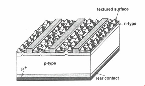
346 Professors Weber and Cuevas-Fernandez and Dr Winderbaum agreed that the known motivations for the development of commercial cells as at November 2007 focussed at one level upon improving the efficiency of the conventional back surface field or BSF structure solar cells. However, they also agreed that:
9. As the front side kept improving, the limitations related to the rear side, in particular the aluminium alloyed highly doped p-type region, or BSF region) [sic] became more obvious, giving rise to the adoption of the so-called PERC solar cell structure. This structure was based on shrinking the aluminium-doped areas to a small fraction of the rear surface and replac[ing] the rest with a surface-passivating dielectric layer (or a stack of layers). By 2007 several research institutions were developing different schemes for passivating the rear side of p-type wafers, including materials like PECVD SiN, SiC and SiOx.
10. As part of that research, it was found that although PECVD SiN provided good passivation of p-type wafers, it caused a “shunting” problem at the solar cell level, as a consequence of its positive charge. …
347 It is apparent that it was known amongst those in the field that there was considerable research activity in the field concerning the development of improved passivation methods, including to the rear of the cell. The development of PERC cells was considered amongst those conducting research in the field to be important in achieving improved efficiencies in solar cell technology. In his oral evidence Professor Cuevas-Fernandez accepted that it was considered that PERC cells would play a “key role”, likely to be considered the “next step” in terms of achieving efficiency.
348 I accept that the common general knowledge included within it awareness of the need to develop an improved means of passivating silicon wafers, including the rear side of p-type wafers for PERC solar cells using materials like PECVD silicon nitride, silicon carbide and silicon oxide.
349 The agreed common general knowledge describes a family of PERC solar cell structures which broadly had the following features:
(a) The same front side as the conventional solar cells, as set out above;
(b) The rear side mostly covered with a passivating dielectric layer, with local openings for the metal contacts;
(c) The entire rear surface covered with a metal; and
(d) The structure (see diagram below) providing improved rear surface passivation and also improved reflective properties.
350 A version of a PERC cell that formed part of the common general knowledge is the PERL cell which had been developed by the University of New South Wales and before November 2007 was known by those skilled in the art to have held the efficiency record for crystalline silicon for some time.
351 The PERL cell was known to have the following features:
(a) Most of the front and rear surfaces of the silicon are passivated by a dielectric film, except for the regions where electrical contact is made; and
(b) The silicon regions underneath the rear contacts are heavily doped while the silicon regions underneath the dielectric film are not.
352 REC Solar submits that the evidence reveals that those in the field were actively interested in finding an alternative to the three known means of passivating the back of the PERC cell. It submits that, in their joint report, Professor Weber and Cuevas-Fernandez and Dr Winderbaum agreed that it was known that PECVD silicon nitride caused shunting in p-type wafers and that the oral evidence demonstrated that it was generally known in the field that thermally grown silicon oxide presented the problem of degrading a multi-crystalline wafer and that PECVD silicon oxide provided inferior interface quality to thermally grown silicon oxide and had not been used in industry.
353 I accept that submission. The experts agreed in their evidence that it was known that thermally grown silicon oxide was used in laboratory settings but that it had the known drawback of degrading a multi-crystalline wafer and they also considered that PECVD silicon oxide did not form the same quality interface as a thermally grown oxide. In those circumstances I accept that there was an interest by those in the field to develop a solar cell with improved surface passivation beyond the existing methods. I consider part of the common general knowledge before November 2007 included an awareness of a desire to confront problems arising from surface passivation consequent upon the reductions in the thickness of multi-crystalline silicon wafers. As the experts agreed, the adoption of the PERC solar structure focussed attention upon the improvement of the passivation of the rear of the cell of p-type wafers.
354 One point of departure between the parties is the extent to which a problem that was known to those engaged in research within the solar cell industry may be understood to be a problem known to the person skilled in the art. Hanwha submits that there is no evidence enabling a sufficiently reliable prediction as to what the person skilled in the art is “likely to have done” or how such a person seeking to make a commercial solar cell would have ascertained Hoex 2006.
355 However, as the agreement between the experts noted above indicates, before November 2007 there was an acknowledged problem facing the solar cell industry that silicon cell efficiency should be increased and cost should be reduced. There were several known strands of research and development under way at that time. Whilst improvements made to the sun-facing side of the conventional solar cell were apparently the main priority, it is clear that there was significant interest in improving the rear surface of PERC cells, and that part of the known problem was to improve the surface passivation of that surface.
356 In this context I do not accept the division that Hanwha seeks to draw between work done by researchers in academic institutions and the work of persons in industry is as stark as Hanwha submits. I have found that the skilled team consists of academic workers as well as persons in industry. They are and were before November 2007 likely to collaborate. Indeed, Dr Winderbaum, himself a worker in industry, gives evidence of his awareness of research being conducted into n-type wafers in academic institutions. Whilst industry workers would not have had an equivalence of knowledge, the evidence indicates that there was likely to have been collaboration between industry and academic institutions in the development of new products. In this regard, it is telling that Dr Winderbaum, whose experience is from the industry side of things, agreed with Professors Cuevas-Fernandez and Weber that the photovoltaic industry had a good record of engaging with research institutions for further investigations, both on immediate topics of interest and in relation to research tasks that required a longer-term view. Professor Cuevas-Fernandez agreed that this included engagement between industry and those research institutions involved in the development of PERC cells.
357 Against the hinterland of common general knowledge research going on before November 2007 the question next arising is whether the person skilled in the art have ascertained Hoex 2006 within the requirements of s 7(3) of the Patents Act.
358 I summarised the test to be applied in Pharmacia LLC at [268]:
The term “ascertain” within s 7(3) of the Patents Act means “to find”: Commissioner of Patents v Emperor Sports Pty Ltd [2006] FCAFC 26; 149 FCR 386 at [30] (Heerey, Kiefel and Bennett JJ). Whether or not the prior art information can be reasonably expected to have been found depends on what the skilled person is likely to have done when faced with a problem similar to that which the patentee claims to have solved with the claimed invention. Section 7(3) requires more than a possibility. It requires a prediction as to the events that would have taken place as at the priority date. The prediction must be sufficiently reliable to be regarded as reasonable: Aspirating IP Ltd v Vision Systems Limited [2010] FCA 1061; 88 IPR 52 at [457] (Besanko J).
359 Hanwha submits that the person skilled in the art would not reasonably be expected to have ascertained Hoex 2006 because there is no evidence enabling a sufficiently reliable prediction as to what that person is likely to have done. It contends that there is no evidence as to how or why the person skilled in the art seeking to make a commercial solar cell would have ascertained Hoex. Nor did Professor Weber conduct what Hanwha submitted was the “usual” theoretical searches when addressing particular problems and REC Solar did not adduce any evidence of any literature search or other search strategy in response to the problem.
360 For a number of reasons, having regard to the known problems in the field at the time as identified above, I am satisfied on the balance of probabilities that the skilled team would be likely to have ascertained Hoex 2006 before November 2006.
361 First, Hoex 2006 was published in Applied Physics Letters, a widely read and respected publication in the photovoltaic field read by those skilled in the art.
362 Secondly, each of Professors Weber and Cuevas-Fernandez and Drs Rentsch and Winderbaum had published articles in that journal, further supporting the evidence that those with the particular focus of their expertise on the development of photovoltaic cells had an interest in that publication and are likely to consult it regularly.
363 Thirdly, Dr Rensch and Professor Cuevas-Fernandez had read the Hoex 2006 article before November 2007. I reject the submission advanced by Hanwha that in so doing they were behaving idiosyncratically because of their particular research interests. Nor do I consider the fact that Professor Weber learnt of the paper shortly after the priority date to be determinative. At the time, he was not engaged in developing different schemes for passivating the rear side of p-type wafers, including materials like PECVD SiN, SiC and silicon oxide.
364 Fourthly, Professor Cuevas-Fernandez gave evidence that at the time he considered that Hoex 2006 was a publication that should be brought to the attention of people because it made a significant contribution.
365 Fifthly, my impression from the evidence is that Hoex 2006 reports a development that was widely hailed to be a significant development of surface passivation, particularly by academic researchers in the field, such that a person with an interest in developing different schemes for passivating silicon wafers would be likely to have heard of and located Hoex 2006 before the priority date.
366 This, in my view, is separately supported by the evidence of the Photovoltaics Literature Survey (No 50), a publication apparently published in 2006 that was tendered in evidence, which identified Hoex 2006 as one of a list of recently published journal articles drawn from a selection of the many articles available from five different publications as one “most relevant” to the Survey’s editorial goal of “helping to keep readers up to date in the field”. Professor Weber used that Survey from time to time to keep up to date. Whilst not determinative, the fact that Hoex 2006 was included within this publication lends support for the submission that Hoex 2006 was likely to have come to the attention of those in the field with an interest in the research reported in it.
367 Finally, I note that, contrary to the implication of Hanwha’s submissions, it is not the case that an artificial ex post facto literature search must be carried out at the time of the conduct of patent litigation in order to establish the “ascertained” aspect of s 7(3) of the Patents Act. Whilst such a search, if properly conducted, may quell controversy about the question, frequently it spawns an enquiry that adds unnecessary expense and argument to an already time consuming aspect of a validity challenge. In the present case, in my view a search of this type was not required because the paper was likely to have been heard of, even if not read, by those skilled in the field.
9.7 Step 3 – would Hoex 2006 be regarded as relevant?
368 In step 3, REC Solar contends that, having ascertained Hoex 2006, the skilled team would learn that the authors had made an important contribution to the development of PERC cells by “rediscovering” the use of aluminium oxide as a passivating layer, demonstrating its excellent passivating qualities in ultrathin layers deposited by ALD on a p-type surface and suggesting its use on the rear surface of a PERC cell.
369 There was no dispute between Professors Weber and Cuevas-Fernandez that the most significant disclosure in Hoex 2006 from the perspective of industrial application was “the ability of Al2O3 to passivate p-type silicon wafers …”.
370 They also agreed that:
It would be obvious, and Hoex 2006 points it out, that Al2O3 [sic] could be an interesting option to passivate the rear surface of the so-called PERC (or PERL) solar cell structure (Structure 2 in Weber aff.# 208).
371 Hanwha submits that the skilled team would not regard Hoex 2006 to be relevant as required by s 7(3) of the Patents Act. However, for the following reasons in my view that submission cannot survive the agreement of the experts.
372 In Lockwood No 2, the High Court said at [153]:
The question of what a person skilled in the relevant art would regard as relevant, when faced with the same problem as the patentee, is to be determined on the evidence. The starting point is the subject matter of the invention to be considered together with evidence in respect of prior art, common general knowledge, the way in which the invention is an advance in the art, and any related matters. It should be mentioned that the starting point is not necessarily the inventive step as claimed, or even agreed between parties, because the evidence, particularly in respect of a combination of integers, may support a different inventive step.
(Emphasis added.)
373 Hanwha submits that when faced with the same problem as the patentee, whilst Hoex 2006 may have been of interest to those in the photovoltaics field generally, it was not relevant to the production of a commercial solar cell. In this regard, it points out that Hoex 2006: (1) does not disclose a firing step; (2) aluminium oxide was not used commercially at the priority date; and (3) the ALD technique used in Hoex 2006 was far too slow to meet the throughput required for mass production of solar cells.
374 However, at the threshold of a publication being regarded as relevant within s 7(3), it is not to the point that Hoex 2006 does not itself disclose a process capable of immediate commercial application. It is plain that the article addresses and proposes a solution to a known problem that researchers in the field considered to be of interest in the development of an improved solar cell for use in future commercial production. The fact that some further work is required to be done does not deprive the article of relevance within s 7(3).
375 It is, of course, another question whether or not, in light of that publication the invention claimed involves an inventive step when considered with the common general knowledge, to which I now turn in the context of the remaining steps in REC Solar’s “pathway”.
9.8 Step 4 – the limits of the teaching in Hoex 2006
376 It will be recalled that one aspect of the manufacture of a typical solar cell before November 2007 involves a firing step whereby the wafer is heated to a temperature of approximately 900 °C for several seconds for the metal contacts. Hoex 2006 does not test the effect of this step on the passivation benefits reported in the use of aluminium oxide on the surface of the wafer.
377 In step 4, REC Solar contends that implementing the suggestion in Hoex 2006 would have involved, as a matter of priority, testing the firing stability of the aluminium oxide layer. That testing would have shown that aluminium oxide was not firing stable. It was reasonable to attribute this, at least in part, to a loss of hydrogen at the interface on firing.
378 Professors Weber and Cuevas-Fernandez and Dr Winderbaum each recognised that the testing of the firing step was absent from Hoex 2006 and that thermal stability studies would be required to test whether the passivation performance of aluminium oxide was stable after firing.
379 REC Solar submits that the skilled team, upon reading the article, would understand that the firing step could have a deleterious effect on passivation, because temperatures of about 900 °C are likely to remove the hydrogen from the silicon nitride layer and thereby change its ability to passivate, its thickness and its reflective index. It submits that the skilled team would conduct thermal stability studies, find that the thin aluminium oxide layers were not firing stable and conclude that a component of the loss of stability was the loss of hydrogen from the interface. From that point, it would have been logical, REC Solar submits, to apply a capping layer to act as a hydrogen reservoir thereby producing a two layer dielectric layer stack.
380 Hanwha submits that REC Solar downplays the difficulties presented in implementing the suggestion in Hoex 2006.
381 In my view the hypothetical skilled team is likely to have faced a number of problems if it decided to move from the teaching of Hoex 2006 to the development of a solar cell.
382 In his affidavit evidence Professor Weber explained:
During the firing process for metal contacts, the aluminium oxide will be subjected to high temperatures of a maximum of approximately 900 °C. The wafer will be at the peak temperature for several seconds. It would therefore have been critical to understand what the firing stability of the aluminium oxide was. If I determined, through the conduct of routine experiments that there was degradation of the passivation effect of aluminium oxide as a result of the firing process, I would have considered whether the aluminium oxide may have reacted with the silicon or whether the structure or composition of the aluminium oxide may have significantly changed in some way (e.g. crystallised). If routine measurements showed that this was not the case, I would most likely have attributed this degradation to there being either insufficient hydrogen in the aluminium oxide or the hydrogen in the aluminium oxide diffusing out of the aluminium oxide too quickly.
383 Professor Weber went on a little later in his affidavit in relation to the thermal stability of aluminium oxide. He said (with line breaks and emphasis added):
If there was degradation of the aluminium oxide during firing, I would have considered whether the aluminium oxide may have reacted with the silicon or whether the structure or composition of the aluminium oxide may have significantly changed in some way (e.g. crystallised).
If routine measurements showed that this was not the case, I would most likely have attributed this to there being either insufficient hydrogen in the aluminium oxide or the hydrogen in the aluminium oxide diffusing out of the aluminium oxide too quickly.
I would therefore have considered combining the aluminium oxide in a stack with another material containing hydrogen that would be available to re-passivate the silicon-aluminium oxide interface during the firing process.
The obvious candidate would have been PECVD silicon nitride, which was a widely used and well-characterised material as at November 2007, and which I knew at November 2007 is a very good reservoir of hydrogen and is compatible with a firing step.
384 The italicised passages above serve to emphasise that Professor Weber was obliged to engage in some conjecture in arriving at his structures 1 and 2. In his oral evidence Professor Weber did not shirk from the experimental obstacles facing the execution of his hypothesis. He accepted that he made two assumptions, one being that upon the firing step there will be degradation and secondly that degradation is not due to a reaction with the silicon or a change in the structure or composition of the aluminium oxide. He said:
MR MURRAY: So this is a completely speculative chain of reasoning, isn’t it?
PROF WEBER: Well, I mean, it is speculative in the sense that it has never been done. I was asked to imagine this. What I’m laying out here, what I’m saying is that, given the information in the Hoex 2006 and 2007 papers, there would have been a chain of experiments, and I mean, I would not have started by making a PERC cell based upon that disclosure, because there were many things that I did not know at the time, and that I would have wanted to know, because they would have informed my further work. So what I’m doing here is laying out the order of the sequence of those steps. I really don’t know how else I can do that.
385 Professor Weber is not to be criticised for taking this approach. In being asked the Hoex 2006 question, he was invited to speculate as to the steps that he would take and he did so.
386 However, it is apparent from his evidence that he advances two alternative hypotheses as to why there may be degradation following firing: (1) insufficient hydrogen and (2) a reaction with the silicon or the structure or composition of the aluminium oxide having significantly changed in some way.
387 In relation to alternative (1), if insufficient hydrogen, Professor Weber considered that could be because of insufficient hydrogen in the aluminium oxide to start with, or alternatively because hydrogen diffused out too quickly upon firing. Professor Weber would then have considered a stack using PECVD silicon nitride as the second layer.
388 In this regard in oral evidence the following exchange had taken place between the experts:
MR LANG: Dr Winderbaum, you've made a comment in your affidavit and I think you said it also to his Honour that the authors in this paper, Hoex 2006, did not test the passivation performance of the layer after a firing step.
DR WINDERBAUM: Correct.
MR LANG: And you were aware as at November 2007 that the high temperature firing step required to fire the contacts of a solar cell could have a significant effect, including an undesirable effect, on the passivating performance of a dielectric structure.
DR WINDERBAUM: Yes.
MR LANG: And did you know why the firing step often produced that result?
DR WINDERBAUM: I have a good guess.
MR LANG: yes.
DR WINDERBAUM: Mainly when you have layers that have a lot of hydrogen in them, by having this high temperature step, most of that hydrogen will disappear, basically. And the layer will become a completely different thing. Change its reflective index, its thickness and its ability to passivate.
PROF WEBER: I agree with – with the comments of Dr Winderbaum.
MR LANG: Thank you. Professor Cuevas?
PROF CUEVAS-FERNANDEZ: Yes, I agree.
389 There is of course a degree of speculation in this evidence. Dr Winderbaum considered that the firing step “could have” a significant adverse effect on passivating performance. He could also make an educated “guess” that the cause of this would be loss of hydrogen. But this speculation tends in my view to over-simplify the type of experimental work required.
390 The evidence disclosed that amongst the variables facing the skilled team is the fact that there was likely to be significant dependence on the thickness of the aluminium oxide layer as to the degree of degradation. There was not a necessary correlation between the degradation results on an experiment replicating the Hoex 2006 work and any degradation resulting in a thinner or thicker layer ultimately used in a commercial product. REC Solar’s evidence did not descend into any detail at all as to the work to be performed in replicating the experiments set out in Hoex 2006.
391 In this regard, Professor Cuevas-Fernandez did accept in his affidavit evidence in response to Professor Weber that the experiments identified by Professor Weber would be the “routine” measurement of the lifetime in a silicon wafer with an aluminium oxide layer deposited on it, before and after firing. Typically firing studies involve measuring the level of passivation without firing and then applying the sort of thermal loads to the structures that they would be subject to during firing and testing passivation performance. But such testing does not of itself reveal the cause of any difference in passivation effect.
392 When Professor Cuevas-Fernandez was asked about post-priority date experiments that involved those tests, which involved testing a range of deposition techniques and a range of conditions and found that the passivation level of aluminium oxide degraded substantially after a firing step, his evidence was that there was a significant dependence on the thickness of the aluminium oxide which meant that relatively thick aluminium oxide layers did not degrade excessively. This leaves room for the fact that, depending on thickness of the aluminium oxide layer, there may not have been relevant degradation at all. Indeed, one variable in outcomes is the degree to which the replication of the home-built plasma ALD experiment reported in Hoex 2006 led to layers of a thickness that was absent degradation.
393 When it was suggested that nonetheless those post-priority date tests determined that one significant reason for the degradation was the loss of hydrogen from the interface, the answer of Professor Cuevas-Fernandez (with whom Professor Weber agreed) was:
PROF CUEVAS-FERNANDEZ: That was harder to establish conclusively. I guess that the simple experiments that you described would not tell us directly if hydrogen loss would be the cause of the degradation, but it was – it was sensible to think that that could be a component of it.
394 In my view this also leaves room for some uncertainty as to whether the skilled team would necessarily arrive at the hypothesis that there was a loss of hydrogen that caused any degradation detected. The evidence indicates that whilst the experiments may have been considered routine, the person skilled in the art would not necessarily conclude that there was a loss of hydrogen (depending on the thickness of the layers deposited in replicating Hoex 2006) and if they did so conclude, would not necessarily conclude in the analysis of the results that the cause, or the sole cause, of the degradation was loss of hydrogen.
395 Alternative (2) identified by Professor Weber is that the cause of any detected degradation may be a reaction with the silicon. He explained in his affidavit that such degradation could have been as a result of a reaction of the aluminium oxide with the silicon during the firing process that may have led to a change in the structure or composition of the aluminium oxide changed, for example crystallised. How this was to be tested was largely unexplored in the evidence adduced by REC Solar. In his affidavit evidence Professor Cuevas-Fernandez questioned whether, as contended by Professor Weber, “routine measurements” would be used to determine whether the aluminium oxide may have reacted with the silicon or whether the structure or composition of the aluminium oxide may have significantly changed in some way. His evidence was that he was not before November 2007 aware of any measurements that he would describe as routine that would be capable of enabling such an assessment. None were any described in the evidence.
9.9 Step 5 – a second dielectric layer?
396 In step 5 REC Solar contends that the testing demonstrating the firing instability of the aluminium oxide layer as a result of a loss, in whole or in part, of hydrogen as identified in step 4 would have led the skilled team to propose PECVD silicon nitride or PECVD silicon oxide as a capping layer, both of which were known hydrogen reservoirs. Determining that they were acceptable would have involved experimentation of a well-known and routine kind.
397 REC Solar submits that Professors Weber and Cuevas-Fernandez agreed that, once the study of thermal stability of single layers of aluminium oxide was completed and showed instability, it would be logical to explore the use of a second layer capping with the aim of improving thermal stability or to provide optical functions in addition to the electronic passivation, choosing first either PECVC silicon nitride (Professor Weber) or PECVD silicon oxide (Professor Cuevas-Fernandez).
398 Hanwha submits that whether or not a stack of aluminium oxide and silicon nitride would be thermally stable was another unknown and that there would have been a concern that depositing silicon nitride may subtract from the beneficial effect of the aluminium oxide by neutralising or decreasing the charge. REC Solar disputes this contention.
399 Professor Cuevas-Fernandez gave evidence that it is not to be taken for granted that silicon nitride would be stable after the firing step, particularly if there is another layer of aluminium oxide beneath it. His view was that one would have to perform careful investigations of the behaviour of those layers. Professor Weber agreed, saying:
PROF WEBER: I think I broadly agree. I don’t know whether you would have needed to be – whether it would have been any more difficult if you’re then now considering a stack rather than a single layer, and you are interested in maintaining the negative charge of that stack. But I certainly agree that … it was necessary to investigate the firing stability of the aluminium oxide film by itself, both with respect to hydrogen and with respect to the negative charge, and that it would have been necessary to do experiments on the stack as well. So I think I would have – if my initial experiments had shown that the charge in the aluminium oxide film was stable, I would have had a reasonably high degree of confidence that a stack – that I would be able to manufacture a stack of aluminium oxide and silicon nitrite that would maintain, also, a negative charge density, but I would not have been 100 per cent sure.
HIS HONOUR: And was there anything that made you think, one way or another, that there would be a stable charge?
PROF WEBER: Not really. I don’t believe my knowledge – because, really, charge, the origin of charge, I think, can be quite complex, and I’m not an expert in it, but I think, in the case of aluminium oxide, the origin of the charge is quite different, for example, from in the case of silicon nitrite, and the Hoex 2006 paper makes mention of the origin of the charge – a speculative mention of it – and so basically, that would have been the basis of my knowledge of it, and so that would not have been enough to tell me, one way or another, I believe.
400 It is apparent that whether the combination proposed by Professor Weber of a double layer of aluminium oxide and silicon nitride represented would work was unknown.
401 Aluminium oxide is negatively charged and silicon nitride is positively charged. Professor Weber said there was nothing one way or the other that made him think that it would form a stable charge. Professor Cuevas-Fernandez said that it would have been a concern that depositing silicon nitride may subtract from the beneficial effect of the aluminium oxide by neutralising or decreasing the charge.
402 Accordingly, assuming in step 4 that interaction between the silicon substrate and the aluminium oxide had been ruled out and assuming that degradation had been detected in navigating step 4 and assuming that the skilled team had reached the conclusion that loss of hydrogen was the cause or a relevant cause of such degradation, then in step 5 Professor Weber would have chosen to use a second dielectric layer of silicon nitride on the assumption that there would not be a deleterious effect on charge.
403 REC Solar answers criticism of Professor Weber’s selection of silicon nitride as a second dielectric layer by reference to the evidence of Professor Cuevas-Fernandez in their joint expert report, where he agrees with Professor Weber that “[o]nce the study of thermal stability of single layers of [aluminium oxide] was completed, it would be logical to explore the use of a second layer capping. The motivation would be to improve the thermal stability of the passivation (if the single [aluminium oxide] layer had proven unstable)”.
404 For the rear side of the PERC cells, such as proposed for structure 2, Professor Cuevas-Fernandez would preferentially pursue PECVD silicon oxide over silicon nitride as a better option. However, that too was predicated on all of the assumptions that arose from the matters considered in step 4.
405 Moreover, the selection of silicon oxide lacked advantages not possessed by silicon nitride, including that silicon oxide was not well known in the industry and it was not known at the time whether or not it would have thermal stability.
9.10 Step 6 – atomic layer deposition
406 Step 6 of REC Solar’s pathway involves an argument drawn from the disclosure of the patent. REC Solar contends that neither the specification nor the claims disclose an invention that concerns a means of applying the aluminium oxide layer using ALD that was fast and efficient enough to be used in a completed industrial process. It contends instead that the method aspect of the invention disclosed and claimed is simply of a means of applying an aluminium oxide layer using ALD that is capable of future industrial application or “industrially feasible”.
407 I accept that the method aspect of the invention disclosed in the patent does not involve the use of ALD to produce a completed and commercially viable first dielectric layer of aluminium oxide as part of a two dielectric layer stack. Nor does it appear to me that Hanwha submitted otherwise. However, in the event that I misapprehend Hanwha’s submissions in this respect I address the argument in brief.
408 The disclosure of the patent is not of an invention of a method using ALD in the deposition of an aluminium oxide layer at any particular speed. ALD was not a process that formed part of the common general knowledge amongst researchers in the photovoltaic industry developing solar cells and the experts agreed that significant work was required to refine any ALD process to develop such a process.
409 The “key” to the method aspect of the invention as described on pages 4-5 and elsewhere did not lie in the particular ALD process, but in the fact that this method enabled, inter alia, a very thin aluminium oxide containing layer to be formed. As each of Professor Weber, Professor Cuevas-Fernandez, Dr Rentsch, Dr Ruby and Dr Glew agreed in the Construction JER, the patent discusses ALD in only general terms and gives some examples of ALD variants (such as remote plasma ALD and thermal ALD) that could be used, but “significant work” would have been required to determine which was most suitable and to design equipment and processes specifically for the industry. In this regard the opening paragraph of the Summary of the Invention says that “it should be possible to produce solar cells displaying very good surface passivation in an economical, industrially viable manner” (emphasis added). The specification does not go further.
410 In this regard, the expert evidence supports the conclusion, which conforms with my understanding, that based on the disclosure of the patent, a researcher who had an ALD reactor and a PECVD reactor would have been able to implement the invention disclosed in a research setting, but it would have taken a number of years and considerable work to implement that invention in an industrial setting, in particular in order to achieve the type of deposition cycle times that would make the process sufficiently swift to be industrially viable.
411 The disclosure of Hoex 2006 pointed the way to the use of the very thin layer aluminium oxide using ALD. Professor Cuevas-Fernandez gave evidence that if he had an ALD reactor he would have been able to implement the disclosure of that publication.
412 So understood, the invention described and claimed does not lie in the production of a commercially viable method of using ALD to produce the first of two dielectric layers.
9.11 Consideration of inventive step
413 By s 7(2) of the Patents Act an hypothetical person skilled in the art, notionally possessed with the common general knowledge as it existed before the priority date, must find the invention to be obvious, whether or not the common general knowledge is supplemented by prior art information within s 7(3): AstraZeneca AB v Apotex Pty Ltd [2015] HCA 30; 257 CLR 356 (AstraZeneca (HC)) at [18] (per French CJ).
414 The law concerning the requirement for an inventive step reflects a balance of policy considerations in patent law of encouraging and rewarding inventors without impeding advances and improvements by skilled, non-inventive persons: Lockwood No 2 at [48] (Gummow, Hayne, Callinan, Heydon and Crennan JJ). The cases over the years have made a number of statements as to what is required to answer the “jury question” of whether or not an invention is obvious. It is a question of fact. The question is not what is obvious to a court, but depends on analysis of the invention as claimed having regard to the state of the common general knowledge, any information relied upon for the purpose of s 7(3), and the approach taken to it by the person skilled in the art: Lockwood No 2 at [51].
415 As a basic premise, the question is always “is the step taken over the prior art an ‘obvious step’ or an ‘inventive step’?” This is often an issue borne out by the evidence of the experts: Lockwood No 2 [52]. Whilst the question remains one for the courts to determine, the courts do so by reference to the available evidence, including that of persons who might be representative of the skilled person in the art: AstraZeneca (HC) at [70] (Kiefel J, as her Honour then was).
416 Various formulations of the question have been set out in the cases. In R D Werner & Co Inc v Bailey Aluminium Products Pty Ltd [1989] FCA 57; 25 FCR 565 at 574, Lockhart J said that there must be “some difficulty overcome, some barrier crossed”.
417 A “scintilla of invention” is sufficient to support the validity of a patent: Aktiebolaget Hässle v Alphapharm Pty Limited [2002] HCA 59; 212 CLR 411 at [48] (per Gleeson CJ, Gaudron, Gummow and Hayne JJ), although this proposition may be seen to be somewhat circular, because the requirement of the qualitative assessment remains that the scintilla so identified must be inventive.
418 In Allsop Inc v Bintang Ltd [1989] FCA 428; 15 IPR 686 at 701 the Full Court (Bowen CJ, Beaumont and Burchett JJ) noted that for the invention to be inventive, it must be “beyond the skill of the calling”.
419 In AstraZeneca (HC), French CJ noted at [15] that relevant content was given to the word “obvious” by Aickin J in Wellcome Foundation Ltd v VR Laboratories (Aust) Pty Ltd [1981] HCA 12; 148 CLR 262 at 286, where Aickin J posed the test:
whether the hypothetical addressee faced with the same problem would have taken as a matter of routine whatever steps might have led from the prior art to the invention, whether they be the steps of the inventor or not.
420 At [15], French CJ (with whom Gageler and Keane JJ and Nettle J agreed) (citations omitted and square brackets in the original) explained:
The idea of steps taken “as a matter of routine” did not, as was pointed out in AB Hässle, include “a course of action which was complex and detailed, as well as laborious, with a good deal of trial and error, with dead ends and the retracing of steps”. The question posed in AB Hässle was whether, in relation to a particular patent, putative experiments, leading from the relevant prior art base to the invention as claimed, are part of the inventive step claimed or are “of a routine character” to be tried “as a matter of course”. That way of approaching the matter was said to have an affinity with the question posed by Graham J in Olin Mathieson Chemical Corporation v Biorex Laboratories Ltd. The question, stripped of references specific to the case before Graham J, can be framed as follows:
“Would the notional research group at the relevant date, in all the circumstances, which include a knowledge of all the relevant prior art and of the facts of the nature and success of [the existing compound], directly be led as a matter of course to try [the claimed inventive step] in the expectation that it might well produce a useful alternative to or better drug than [the existing compound]?”
That question does not import, as a criterion of obviousness, that the inventive step claimed would be perceived by the hypothetical addressee as “worth a try” or “obvious to try”. As was said in AB Hässle, the adoption of a criterion of validity expressed in those terms begs the question presented by the statute.
421 The approach proposed by Graham J in Olin Mathieson Chemical Corporation v Biorex Laboratories Ltd [1970] RPC 157 to which French CJ refers is often referred to as the “modified Cripps question”. The application of the modified Cripps question has been the subject of recent consideration. In Generic Health Pty Ltd v Bayer Pharma Aktiengesellschaft [2014] FCAFC 73; 222 FCR 336, the Full Court said at [71] (Besanko, Middleton and Nicholas JJ) (emphasis added):
We do not think that the plurality in Alphapharm were saying that the reformulated Cripps question was the test to be applied in every case. Rather, it is a formulation of the test which will be of assistance in cases, particularly those of a similar nature to Alphapharm. The plurality did not reject as an alternative expression of the test the question whether experiments were of a routine character to be tried as a matter of course (The Wellcome Foundation Limited v VR Laboratories (Aust) Proprietary Limited (1981) 148 CLR 262, at 280-281, 286, per Aickin J). We do not think there is a divide here in terms of whether an expectation of success is relevant between a test which refers to routine steps to be tried as a matter of course and the reformulated Cripps question. It is difficult to think of a case where an expectation that an experiment might well succeed is not implicit in the characterisation of steps as routine and to be tried as a matter of course. On the other hand, we think a test formulated in terms of worthwhile to try was firmly rejected by the High Court in Alphapharm (see also Pfizer, at 476, [287], per French and Lindgren JJ [Pfizer Overseas Pharmaceuticals v Eli Lilly and Co (2005) 225 ALR 416]). The fact (if it be the fact) that the position in the United States may have shifted does not affect the binding nature of what the plurality said in Alphapharm.
422 In Nichia Corporation v Arrow Electronics Australia Pty Ltd [2019] FCAFC 2, the Full Court (Jagot J, with Besanko and Nicholas JJ agreeing) picked up on the emphasised passage in concluding that, in finding that there were “a number of unknowns” and that the patentee “did not know” that a combination would produce a satisfactory result within the claim, the primary judge strayed from “the test of steps taken in an expectation that they might well produce the invention or a useful result towards a test of an expectation of knowing that steps will produce a useful result based on predictive capacity” (at [88]-[89]). The relevant test is merely expecting that the steps may well work, rather than knowing that steps will or would or even may well work (at [99]).
423 In relation to having multiple avenues to try, in Nichia the Full Court adopted as orthodox the statement of Laddie J in Brugger v Medic-Aid Ltd [1996] WLUK 122; RPC 635 at 661:
… if a particular route is an obvious one to take or try, it is not rendered any less obvious from a technical point of view merely because there are a number, and perhaps a large number, of other obvious routes as well. If a number of obvious routes exist it is more or less inevitable that a skilled worker will try some before others. The order in which he chooses to try them may depend on factors such as the ease and speed with which they can be tried, the availability of testing equipment, the costs involved and the commercial interests of his employer. There is no rule of law or logic which says that only the option which is likely to be tried first or second is to be treated as obvious for the purpose of patent legislation.
424 In Insta Image Pty Ltd v KD Kanopy Australasia Pty Ltd [2008] FCAFC 139; 239 FCR 117 at [80] (Lindgren, Bennett and Logan JJ), the Full Court considered lack of inventive step in the context of the Patents Act. It held at [80] that, in determining the issue of obviousness it was necessary:
(1) to identify the invention “so far as claimed in any claim”;
(2) to identify the “person skilled in the relevant art”;
(3) to identify the common general knowledge as it existed in Australia before the priority date;
(4) to inquire under s 7(2) whether the invention referred to in (1) above would have been obvious to the person referred to in (2) above in light of the knowledge referred to in (3) above; and
(5) to inquire whether that invention would have been obvious to that person in the light of that knowledge when that knowledge is considered together with either kinds of information mentioned in s 7(3) (additional prior art information).
9.11.2 Analysis of lack of inventive step
425 REC Solar has advanced its case based on lack of inventive step by reference to the six steps of the pathway that I have described in some detail in sections 9.6 – 9.10 above. There is a seductive simplicity in the manner in which REC Solar advances its case which tends to belie the obstacles that lay in the way of the skilled team in advancing from the common general knowledge, when supplemented by Hoex 2006, to the invention as claimed.
426 In this regard it may be recalled that claim 9, which is the broadest of the claims challenged for want of inventive step, is in the following form:
9. Solar cell comprising: a silicon substrate (1): a first dielectric layer (3) comprising aluminium oxide on a surface of the silicon substrate (1) wherein the first dielectric layer has a thickness of less than 50nm, preferably less than 30nm and more preferably less than 10nm; a second dielectric layer (5) on a surface of the first dielectric layer (3), the materials of the first and second dielectric layer differing and hydrogen being embedded into the second dielectric layer.
427 As broadly summarised, it is for a solar cell including a silicon substrate, a first dielectric layer comprising aluminium oxide of a specified thickness range and a second dielectric layer on the surface of the first of a different material having hydrogen embedded into it.
428 In reviewing the steps along the pathway, I have explained in relation to steps 1, 2 and 3 my view that the skilled team would have been aware of the relevant problem and have ascertained, understood and regarded Hoex 2006 as relevant. However, I do not consider that REC Solar has established that it was obvious to move through steps 4 and 5 to the invention as claimed. That aspect of the pathway involved, as I have noted, assuming in step 4 that interaction between the silicon substrate and the aluminium oxide had been ruled out using unspecified tests and unspecified analysis the form of which the hypothetical worker or team was unaware; assuming that degradation had been detected when conducting tests on the aluminium oxide layer when varying thicknesses of layers were used and assuming that the skilled team had reached the conclusion that a loss of hydrogen (if any) was the cause or a relevant cause of such degradation and then in step 5 choosing a second dielectric layer of silicon nitride on the assumption that there would not be a deleterious effect on charge.
429 I accept that in some cases a series of routine tests with predictable outcomes may yield a conclusion that the movement from the prior art base to the invention claimed does not involve an inventive step. An example may be seen in Merck Sharp & Dohme at [828] (Burley J). However, I consider that on balance the position in the present case is different. I consider that the series of tests proposed by Professor Weber in his hypothetical exercise, as elucidated by reference to the whole of the evidence, reveals a series of decisions was required to move in steps 4 and 5 from the single layer of aluminium oxide as taught in Hoex 2006 to the two layered stack of the invention such that the line was crossed between there being a case where the steps could be seen as routine to try as a matter of course to a case where, in my view, the skilled team was simply postulating steps which would be worthwhile to try, of the type rejected by the High Court in Alphapharm.
430 As a consequence, in my view REC Solar has not demonstrated that the invention of claim 9 lacks an inventive step. The same conclusion applies to all of the challenged claims which are dependent on claim 9.
9.12 Inventive step in light of Hoex 2007
431 Hoex 2007 is entitled “Excellent passivation of highly doped p-type Si surfaces by the negative-charge-dielectric layer Al2O3”.
432 Several of the authors also contributed to Hoex 2006 and the lead author, Dr Hoex, is the same for both. Hoex 2007 was also published in Applied Physics Letters. It was received by the editors on 6 July 2007, accepted for publication on 21 August 2007 and published online on 11 September 2007.
433 REC Solar relies on Hoex 2007 as a standalone document forming part of the prior art base within s 7(3) of the Patents Act that, when considered together with the common general knowledge, would sufficiently arm the skilled team to lead to the invention claimed in the patent in a manner that lacks an inventive step within s 7(2).
434 Professor Weber was provided with a copy of Hoex 2007 and asked to comment on its disclosure. In contrast with Hoex 2006, Hoex 2007 does not address the passivation of the most common p-type silicon wafer with an n-type emitter at the front (sun-facing) side of the solar cell, which was used in the Conventional Solar Cell structure. Rather, it addresses the passivation of an n-type silicon wafer which has a p-type emitter. Professor Weber explains that the paper discloses that aluminium oxide films were deposited on both sides of each of the silicon samples using a remote plasma ALD reactor, resulting in a layer of aluminium oxide that was 30 nm thick being deposited on both sides of the wafer. It shows that aluminium oxide was significantly better performing as a passivating layer than other materials on heavily p-doped, diffused silicon surfaces. As with Hoex 2006, in Hoex 2007 the authors did not use a firing step where the wafers with the aluminium oxide layer were subjected to elevated temperatures of about 900 °C.
435 In the inventive step JER, Professors Weber and Cuevas-Fernandez and Dr Winderbaum agreed that the main disclosures in Hoex 2007 were:
Excellent passivation of boron diffused emitters (that is, heavily boron doped, p-type surfaces) demonstrated by ALD deposited aluminium oxide films;
Both the negative charge density in the aluminium oxide film as well as a low density of interface defects are responsible for the excellent passivation, even though the paper does not mention the possible presence of hydrogen in the aluminium oxide film; and
Achievement of the excellent passivation requires a post-deposition anneal at around 400-500 °C.
436 After summarising in some detail the disclosure of Hoex 2007, Professor Weber was then asked the Hoex 2007 question and gives the opinion that he would have been directly led to try each of structures 1 and 2. He considers that it would have been straightforward to implement both in a research laboratory, however he considers that structure 2 would have provided an easier transition from the existing commercial technology at the time than structure 1.
437 Professor Weber then explains in his affidavit his rationale for adopting this approach. Significantly, he says that he would use the same approach in determining the effects of the firing step upon the aluminium oxide layer as he would in relation to Hoex 2006, as I have discussed in some detail in relation to steps 4 and 5 in sections 9.8 and 9.9 above. Professor Cuevas-Fernandez provides the same criticisms and the evidence in the IS JER and oral evidence in relation to these matters is equally applicable.
438 REC Solar proposes a five step pathway to the conclusion that the invention claimed lacks an inventive step by virtue of the disclosure of Hoex 2007:
(1) In the years prior to November 2007, developing an efficient solar cell using an n-type wafer was a subject of research interest, and was also of niche industry interest. That was so because n-type wafers had better tolerance of impurities, but were higher in cost.
(2) It was commonly known by researchers that the passivation performance of silicon oxide and silicon nitride on n-type wafers having p+ emitters was trailing behind their performance on the surface of p-type silicon having n+ emitters.
(3) Hoex 2007 was an extension of the work of Hoex 2006 and, this time, demonstrated excellent passivation performance of aluminium oxide on a p+ surface. It suggested use as a passivation layer on an n-type wafer.
(4) Given the importance of the optical properties at the front of the solar cell and the relatively low refractive index of aluminium oxide, if would have been immediately apparent that a capping layer with a higher refractive index was necessary. Similarly to Hoex 2006, implementing the disclosure in Hoex 2007 would have also necessitated firing stability tests. These considerations would have led to proposing a silicon nitride capping layer.
(5) Developing industrially viable processes for the processing of n-type wafers (including diffusion and metallisation) may have taken considerable work, but the same work would have been required to implement the patent, which discloses no more than that the dielectric structure can be implemented on n-type silicon. In both cases, that work would have been lengthy, but would not have required invention.
439 It will be noted that step 4 includes the substance of steps 4 and 5 for the Hoex 2006 pathway, including the requirements that implementing Hoex 2007 would involve firing stability tests and a decision in relation to a second capping layer. It is these steps that I have determined yield the result that REC Solar has not established that the invention in the challenged claims lacks an inventive step.
440 Accordingly, the conclusion that I have reached in relation to Hoex 2006 is equally applicable to the case advanced by REC Solar in relation to Hoex 2007.
10.1 Relevant law of fair basis
441 Section 40(3) provides:
The claim or claims must be clear and succinct and supported by matter disclosed in the specification.
442 In Lockwood Security Products Pty Ltd v Doric Products Pty Ltd [2004] HCA 58; 217 CLR 274 (Lockwood No 1) the High Court identified what has become the seminal test for lack of fair basis:
68 Erroneous principles. The comparison which s 40(3) calls for is not analogous to that between a claim and an alleged anticipation or infringement. It is wrong to employ “an over meticulous verbal analysis”. It is wrong to seek to isolate in the body of the specification “essential integers” or “essential features” of an alleged invention and to ask whether they correspond with the essential integers of the claim in question.
69 “Real and reasonably clear disclosure”. Section 40(3) requires, in Fullagar J’s words, “a real and reasonably clear disclosure.” But those words, when used in connection with s 40(3), do not limit disclosures to preferred embodiments.
“The circumstance that something is a requirement for the best method of performing an invention does not make it necessarily a requirement for all claims; likewise, the circumstance that material is part of the description of the invention does not mean that it must be included as an integer of each claim. Rather, the question is whether there is a real and reasonably clear disclosure in the body of the specification of what is then claimed, so that the alleged invention as claimed is broadly, that is to say in a general sense, described in the body of the specification.”
Fullagar J’s phrase serves the function of compelling attention to the construction of the specification as a whole, putting aside particular parts which, although in isolation they might appear to point against the “real” disclosure, are in truth only loose or stray remarks.
10.2 Ground 5 – the ALD argument
443 REC Solar contends that the challenged claims travel beyond the matter described in the specification in that there is no real and reasonably clear disclosure in the specification of a solar cell, or a method for manufacturing such a solar cell, having a first dielectric layer formed by means other than ALD.
444 In its submissions, REC Solar observes that the claims identified are product claims which do not require the first dielectric layer to be deposited by ALD. It submits that this has the consequence that those claims are not fairly based because there is no disclosure in the specification of an invention in which the first dielectric layer comprising aluminium oxide is deposited by any means other than ALD. Citing AstraZeneca FFC at [421] (Besanko, Foster, Nicholas and Yates JJ), it contends that the specification does not make any such disclosure, even in a general sense. Rather, it teaches that the invention is a particular method of manufacturing a solar cell using ALD to deposit the first dielectric layer. This, it submits, is consistent with an agreement of Professors Weber and Cuevas-Fernandez.
445 REC Solar also draws heavily on disclosures in the specification that the “idea” upon which the invention is based includes forming the first dielectric layer by ALD; that a “key to understanding the outstanding passivating effect” is the “combination of the Si/Al2O3 interface, which is ideally atomically flat and is produced as a matter of course during the ALD process”; that an “essential advantage” of ALD is the “fact that the entire substrate surface is coated uniformly”; and that it is the “combination according to the invention of the two known deposition methods, ALD and PECVD” which creates a passivating layer which is “optimally suitable”. It contends that the overall structure and content of the specification underscores these matters and that on no view can the consistory clause be regarded as providing a real and reasonably clear disclosure. Finally it draws on the expert evidence as supporting the view that it submits can be drawn from the specification.
446 Hanwha contends that the invention in the challenged claims is adequately disclosed in the specification.
447 The question of whether there is a real and reasonably clear disclosure in the specification of what is then claimed requires consideration of whether it is appropriate to say that in a general sense the invention of claim 9 is described in the body of the specification. REC Solar’s argument focusses on the absence of any requirement in that claim that the first dielectric layer be deposited by ALD.
448 Review of the disclosure of the specification through the eyes of the person skilled in the art leads me to the view that REC Solar’s argument cannot succeed because it is apparent from the specification that the invention asserted by the patentee includes a product absent the requirement that it be manufactured by any particular method. As noted in Lockwood No 1 at [69], fair basis concerns what the patentee asserts the invention to be.
449 Turning to the disclosure of the specification (which I have addressed more fully in section 5 above), the Field of the Invention notes that it relates to a method for manufacturing a solar cell “with a surface passivating dielectric double layer” and to a “corresponding solar cell”, thereby identifying the method and the product aspects of the invention which share as their common feature the dielectric double layer. Nothing in this language requires that the corresponding solar cell be made in accordance with any particular method.
450 The Background of the Invention commences by reference to the key requirement for solar cells that they have effective suppression of surface recombination losses and then goes on to identify how the prior art has addressed this requirement by the four different approaches to which I have referred in section 5.1 above. In three of the four approaches, not only a manufacturing process is identified but also a consequence of that process on the viability of the product of that process. Thus for the first there is a problem with the charge carrier lifetime (page 2 lines 4-5), the second the pinhole and parasitic shunt problems (page 2 lines 15-24) and for the third the potential for degradation of the passivating effect of amorphous silicon layers (page 3 lines 7-13).
451 The Summary of the Invention states that there is a need for a solar cell and a method for manufacturing a solar cell in which good passivation of the surface can be achieved and also at least partial avoidance of the drawbacks of the conventional layers can be avoided (page 3 line 28 to page 4 line 2). As noted, those drawbacks are not confined to those involved in the manufacture of solar cells. The need is said to be met by the subject matter of the claims, thereby directing attention not only to the method of claim 1, but the product of claim 9.
452 The specification then in detail describes the first aspect of the invention which concerns the method which includes the use of ALD for the deposition of the first dielectric layer. The “idea” of the method is a method for manufacturing silicon solar cells whereby (page 4 lines 19-23):
… The dielectric passivating layer is composed of two partial layers, of a very thin aluminium oxide-containing layer, which is formed by atomic layer deposition (ALD), and also of a thicker layer made of silicon oxide, silicon nitride or silicon carbide, for example, which can be deposited on the aluminium oxide layer by means of plasma enhanced chemical vapour deposition (PECVD), for example.
453 Two concepts emerge from this. One is that a first, very thin layer of aluminium oxide is formed by ALD and a second thicker layer may, for example be deposited by PECVD. The second is that a two dielectric layer stack is being formed.
454 A paragraph later at page 5 lines 10 to 16, the specification refers to the “key” to understanding the outstanding passivation effect and tempering stability of the stack layer according to the invention which:
… may be identified in the combination of the Si/Al2O3 interface, which is ideally atomically flat and is produced as a matter of course during the ALD process, and the highly hydrogenous SiOx, SiNx or SiCx layers, such as are formed during the PECVD process, for example. A part of the hydrogen from the PECVD-deposited layers can diffuse through the ultrathin Al2O3 layer and passivate unsaturated silicon bonds at the interface to the silicon.
455 It may be seen that the same two concepts are further developed. First that the Si/Al2O3 interface which is “ideally” flat and produced by the ALD process and that highly hydrogenous SiOx, SiNx or SiCx layers formed using PECVD (as an example) can provide hydrogen to interact with the silicon bonds at the interface. The second is more generally that the combination of the Si/Al2O3 interface (the first layer) and the highly hydrogenous SiOx, SiNx or SiCx layer (the second layer) has the beneficial effect of enabling the hydrogen to diffuse through the ultrathin first (Al2O3) layer.
456 Contrary to the submission advanced by REC Solar, nothing in this passage mandates that the beneficial effects of the invention can only be obtained by the use of ALD in the deposition of the first layer or that ALD is “essential” to the invention. The passage is manifestly directed to the method aspect of the invention. Nor, in my view, may it be said that the statement that “[a]n essential advantage of [ALD] is the fact that the entire substrate is coated uniformly” makes the use of ALD essential to the invention as described and disclosed in the specification. That passage is describing an inherent advantage of ALD, not an essential advantage of the invention as a whole.
457 The specification at page 9 line 28 to page 10 line 3 provides expressly for the second aspect of the invention in a consistory clause the terms which substantially match claim 9. The passage identifies the use of two dielectric layers, one of aluminium oxide and the other with hydrogen embedded in it. In the paragraph that follows, the specification notes that features and advantages of the invention have been described mainly in relation to the manufacturing method, but a person skilled in the art:
… will recognise both from the foregoing and from the subsequent description that, unless otherwise indicated, the embodiments and features of the invention are also transferable by analogy to the solar cell according to the invention. In particular, the features of the various embodiments may also be combined with one another in any desired manner.
458 Informed by this statement, in my view the person skilled in the art would readily distil from the description of the method aspect that the invention insofar as it related to the product claim is said to lie in the second of the concepts to which I have referred above, namely the use of a two layer stack, a thin first layer comprising aluminium oxide and the second layer with hydrogen embedded in it. Those aspects of the description of the method are neutral as to the means by which the dielectric layers are formed.
459 Furthermore, it may be noted that the specification does not here assert that the solar cell of the second aspect must be made in accordance with the method described. To the contrary, the features of the invention are said to be only transferrable “by analogy” to the solar cell – thereby indicating an assertion on the part of the patentee that its invention lies in the product per se, regardless of how it is made.
460 This view is supported by fact that in the summary provided at page 10 line 13 to page 11 line 6 the specification asserts that the method or solar cell according to aspects of the invention is to be distinguished from previously known methods for the surface passivation of solar cells in terms of five points, none of which rely on the use of ALD as a point of distinction. It is true that the summary provided at the conclusion of the specification at page 13 line 18 to page 14 line 11 is directed towards the method aspect of the invention, but nothing in that summary can be read to detract from the earlier disclosures, or to suggest that the invention solely resides in the method described. In this regard, the position is not analogous to any of Olin Corporation v Super Cartridge Co Pty Ltd [1977] HCA 23; 180 CLR 236 as described in Lockwood No 1 at [98], Atlantis Corporation Pty Ltd v Schindler [1997] FCA 1105; 39 IPR 29 as described in Lockwood No 1 at [87] or Sigma Pharmaceuticals (Australia) Pty Ltd v Wyeth [2011] FCAFC 132; 119 IPR 194.
461 REC Solar submits that the consistory clause relied upon by Hanwha does not provide a real and reasonably clear disclosure of a solar cell in which the first dielectric layer is deposited by means other than ALD. It contends that the passage on page 9-10 on its face is directed to a “second aspect of the invention” which is, it says, the “same invention” as the first aspect, which requires the use of ALD and that as such, even read literally, the specification does not disclose a solar cell manufactured by any other method than that described in the first aspect. For the reasons given, in my view this does not accord with a fair reading of the specification.
462 Nor, in my view, can agreement of the experts that the specification repeatedly teaches the use of ALD to deposit the first dielectric layer comprising aluminium oxide and discloses no other means of deposition the first layer be determinative. Whilst it is true (as the experts agreed) that significant parts of the specification concern the use of ALD when describing the first aspect of the invention and that ALD had not hitherto been a part of the common general knowledge in the context of the deposition of such dielectric layers, the question of fair basis is resolved by having regard to the quality of the disclosure, not the quantity; Idenix Pharmaceuticals LLC v Gilead Sciences Pty Ltd [2017] FCAFC 196; 134 IPR 1 at [326] (Nicholas, Beach and Burley JJ). The more detailed description of ALD is explicable because it was not a mainstream process for deposition of such dielectric layers, but that conclusion is not inconsistent with the use of ALD being confined to the first aspect of the invention.
463 I am satisfied that there is nothing in the body of the specification to suggest that the description of the invention found in the consistory clause on pages 9-10 is wider than the invention stated in the specification. I accept that to couch a claim “in the same terms as the description of the invention in the specification” does not of itself, by that mere “coincidence of language”, establish fair basing; Lockwood No 1 at [87]. If part of the language of the specification does not reflect the description of the invention in the light of the specification as a whole, then the claim will not be fairly based. Nevertheless, it is customary for the consistory clause to describe the invention in its broadest form and that a consistory clause may provide fair basis for a claim that uses the same language; AstraZeneca FFC at [419]. In the present case, in the specification it is not only the consistory clause but also the other passages in the specification to which I have adverted that persuade me that, at least in this respect, claim 9 (and the identified dependent claims) are fairly based.
10.3 Grounds 6, 7 and 8 “on a surface”
464 Each of grounds 6, 7 and 8 depend upon the outcome of the dispute concerning the construction of integer 9(c) in claim 9 which concerns the location of a first dielectric layer “on a surface of the silicon substrate”. If this integer is construed to mean, as REC Solar contends (and as I have found), that no layer may be formed on the silicon substrate prior to the deposition of the aluminium oxide layer, then these grounds have no work to do. However, if the language of the claims is taken to embrace methods or products which involve forming a layer of silicon oxide on the silicon substrate then the claims are not fairly based for the reason that, as a chemically passivating layer used as the first layer in a stack (such as silicon oxide) becomes thicker, there is a trade-off between the increasing chemical passivation against the decreasing field passivating effect of a field-effect passivating layer (such as aluminium oxide) as it becomes more distant from the silicon substrate.
465 I have in section 6 concluded that REC Solar’s submission as to the construction of integers 1(c) and 9(c) is correct. Accordingly, grounds 6, 7 and 8 do not arise for consideration.
466 Section 18(1)(b)(i) of the Patents Act requires that an invention, so far as claimed in any claim, when compared to the prior art base, be novel.
467 The touchstone for lack of novelty is whether a prior publication anticipates a claimed invention. In General Tire at 485-486, Sachs, Buckley and Orr LJJ said:
When the prior inventor’s publication and the patentee’s claim have respectively been construed by the Court in the light of all properly admissible evidence … the question whether the patentee’s claim is new … falls to be decided as a question of fact. If the prior inventor’s publication contains a clear description of, or clear instructions to do or make, something that would infringe the patentee’s claim if carried out after the grant of the patentee’s patent, the patentee’s claim will have been shown to lack the necessary novelty, that is to say, it will have been anticipated. The prior inventor, however, and the patentee may have approached the same device from different starting points and may for this reason, or it may be for other reasons, have so described their devices that it cannot be immediately discerned from a reading of the language which they have respectively used that they have discovered in truth the same device; but if carrying out the directions contained in the prior inventor’s publications will inevitably result in something being made or done which, if the patentee’s patent were valid, would constitute an infringement of the patentee’s claim, this circumstance demonstrates that the patentee’s claim has in fact been anticipated.
If, on the other hand, the prior publication contains a direction which is capable of being carried out in a manner which would infringe the patentee’s claim, but would be at least as likely to be carried out in a way which would not do so, the patentee’s claim will not have been anticipated, although it may fail on the ground of obviousness. To anticipate the patentee’s claim the prior publication must contain clear and unmistakable directions to do what the patentee claims to have invented … a signpost, however clear, upon the road to the patentee’s invention will not suffice. The prior inventor must be clearly shown to have planted his flag at the precise destination before the patentee.
468 In considering the question of whether a prior publication anticipated the claims of a patent, the Full Court in AstraZeneca FFC referred to the reverse infringement test in Meyers Taylor Pty Ltd v Vicarr Industries Ltd [1977] HCA 19; 137 CLR 228 at 235 (Aickin J) and also the observations in Flour Oxidizing Company Ltd v Carr & Co Ltd [1908] 25 RPC 428 at 457 of Parker J to the effect that it is not enough to prove that an apparatus described in an earlier specification could have been used to produce a result, it must also be shown that the specification contains clear and unmistakable directions to do so. In that context the Court in AstraZeneca said:
301 These observations are the wellspring of a long line of cases that recognise that, in order for a prior art document to be anticipatory, there must be (to adopt the language in General Tire) a clear description of, or clear instructions to do or make, something that would infringe the patentee’s claim if carried out after the grant of the patentee’s patent. In Bristol-Myers Squibb Company v F H Faulding & Co Limited (2000) 97 FCR 524 (“Bristol-Myers”), Black CJ and Lehane J reviewed the relevant authorities and concluded (at [67]):
What all of those authorities contemplate, in our view, is that a prior publication, if it is to destroy novelty, must give a direction or make a recommendation or suggestion which will result, if the skilled reader follows it, in the claimed invention. A direction, recommendation or suggestion may often, of course, be implicit in what is described and commonly the only question may be whether the publication describes with sufficient clarity the claimed invention or, in the case of a combination, each integer of it. …
(Emphasis added.)
469 REC Solar contends that Isaka anticipates claims 9, 11-14, 17-19 and 21 of the patent.
470 Isaka is a PCT application as defined in Schedule 1 of the Patents Act. Section 7(1)(c) of the Patents Act provides that an invention is taken to be novel when compared with the prior art base unless it is not novel in light of prior art information contained in a single specification of the kind mentioned in (b)(ii) of the definition of prior art base in Schedule 1.
471 The definition of prior art base relevantly provides:
…
(b) in relation to deciding whether an invention is or is not novel:
…
(ii) information contained in a published specification filed in respect of a complete application where:
(A) if the information is, or were to be, the subject of a claim of the specification, the claim has, or would have, a priority date earlier than that of the claim under consideration; and
(B) the specification was published after the priority date of the claim under consideration; and
(C) the information was contained in the specification on its filing date and when it was published.
472 As a result of admissions made by Hanwha, there is no dispute that the requirements of (b)(ii)(B) and (C) are satisfied. Accordingly, the information disclosed in Isaka will form part of the prior art base if (b)(ii)(A) is met. In this regard, there is no dispute that the priority date of Isaka is 1 December 2006.
473 One potentially relevant issue is whether, if the information disclosed in Isaka were to be the subject of a claim, it would have a priority date earlier than that of the patent (being 7 November 2007). The question of priority date is addressed by s 43(2) of the Patents Act which provides that the priority date is determined by the date of filing of the specification or as provided in the regulations. REC Solar contends that the information contained in Isaka would have a priority date earlier than the patent because the information upon which they rely for the purposes of their novelty argument is or would be the subject of a claim entitled to a priority date earlier than the priority date of the claims in the patent. For that purpose it has supplied a set of notional claims with their closing submissions. However, Hanwha does not take issue with the contention that Isaka is a relevant priority document and also accepts that the question of novelty is answered one way or the other entirely by consideration of the disclosure of Isaka. Accordingly, it will not be necessary to consider the question of whether the notional claims are fairly based on the disclosure of Isaka.
474 Isaka is a Japanese patent application which was translated for the purposes of these proceedings. Professors Cuevas-Fernandez and Weber addressed their areas of agreement and disagreement in the Validity JER.
475 There is a limited contest between the parties as to what integers of the claims are not disclosed.
476 In relation to claim 9, the parties are at odds as to whether:
(a) Integer 9(c): “first dielectric layer comprising aluminium oxide” is disclosed; and
(b) Integer 9(d): “wherein the first dielectric layer has a thickness of less than 50 nm, preferably less than 30 nm and more preferably less than 10 nm” is disclosed;
Otherwise, Hanwha accepts that if claim 9 is disclosed, then the additional integers in claims 11, 14, 17-18 and 21 are disclosed insofar as they are dependent on claim 9. It raises the following separate arguments in relation to further integers in claims 12, 13 and 21.
477 In relation to claim 12, the parties are at odds as to whether the additional integer “the second dielectric layer has a thickness of more than 50 nm, preferably more than 100 nm and more preferably more than 150 nm” is disclosed.
478 In relation to claim 13, the parties disagree as to whether or not the integer “the second dielectric layer has a thickness of more than 100 nm” is disclosed.
479 In relation to claim 19, the parties agree that, having regard to the construction that I have adopted of the words “back surface reflector”, this integer is disclosed.
11.2.3 The disclosure of Isaka
480 Isaka is entitled “Solar Cell and Manufacturing Method Therefor” and identifies the field as being the same. It first describes the Background Art. Next, under the heading “Problem to Be Solved by the Invention”, the following passages are of particular relevance:
0007 A silicon oxide film is typically used as a silicon substrate back surface passivation film in a solar cell. A silicon oxide film, particularly a silicon oxide film formed using a thermal oxidation method (hereinafter also referred to as a thermal oxide film), has a strong passivation effect and is thus widely used as a solar cell passivation film. However, because thermal oxide films have different deposition rates depending on silicon substrate impurity concentration, said films are prone to film thickness unevenness depending on silicon substrate condition.
0008 Meanwhile, a relatively strong passivation effect can be achieved by forming a silicon nitride film on a back surface of a silicon substrate in a solar cell, albeit not as strong a passivation effect as achieved with a thermal oxide film. Furthermore, unlike a thermal oxide film, a silicon nitride film can be formed at a uniform thickness regardless of silicon substrate condition. Furthermore, said film has high resistance to hydrogen fluoride used in a solar cell manufacturing process.
0009 However, a silicon nitride film has a fixed positive charge and is thus considered unsuitable for use as a passivation film for a p region in a solar cell.
0010 Based on the problem described above, an object of the present invention is to provide a solar cell on which is formed a passivation film having a strong effect in both a p region and an n region on a back surface of a silicon substrate in the solar cell.
Means for Solving Problem
0010 The present invention relates to a solar cell on which a first passivation film made of a silicon nitride film is formed on a surface opposite a light receiving surface of a silicon substrate, wherein a refractive index of the film is 2.6 or more.
0011 The present invention relates to a solar cell on which a first passivation film made of a silicon nitride film is formed on a surface opposite a light receiving surface of a silicon substrate, wherein a refractive index of the film is 2.6 or more.
0012 Furthermore, it is preferable that the solar cell according to the present invention is a back surface junction-type cell with a pn junction formed on the surface opposite the light receiving surface of the silicon substrate.
0013 Furthermore, it is preferable that the solar cell according to the present invention have a second passivation film, formed between the silicon substrate and the first passivation film, the second passivation film including a silicon oxide film and/or an aluminum oxide film.
…
(Emphasis added.)
481 There is no dispute that the reference to “films” may be understood to mean “layers” or that the word “aluminum” means “aluminium”. Nor is it in dispute that the “second passivation film” identified in [0013] (and also later) equates to the “first dielectric layer” of claim 9 inasmuch as it is described as being placed between the silicon substrate and the silicon nitride layer.
482 Isaka includes as figure 2 the following diagram of a solar cell in cross-section:
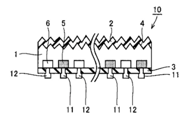
483 In describing the structure of the solar cell at [0029], the solar cell (10) of a preferred embodiment is said to include a back surface junction-type solar cell wherein a silicon substrate (1) is used as a material and a plurality of p+ layers (5) and n+ layers (6) are formed alternately at intervals on the back surface of the substrate. In addition, p electrodes (11) and n electrodes (12) are formed on the p+ layers (5) and n+ layers (6) respectively. The back surface where (11) and (12) are not formed is covered with a passivation film (3). Isaka goes on:
0029 … Here, the passivation film (3) according to the present invention includes both that formed only from a first passivation film and that formed from a laminate of the first passivation film and a second passivation film (not illustrated in the drawings). …
…
0030 As illustrated in FIG.2, the passivation film 3 is formed on the back surface of the silicon substrate 1. A structural pattern of the passivation film 3 according to the present invention has either one of the two following forms, (1) and (2).
(1) A pattern where only the first passivation film is formed on the back surface of the silicon substrate 1 as the passivation film 3.
(2) A pattern where the second passivation film is formed on the back surface of the silicon substrate 1, and then, the first passivation film is formed thereupon as the passivation film 3.
0031 That is, in the case of (2) described above, a second passivation film is formed between the back surface of the silicon substrate 1 and the first passivation film. When being formed, the second passivation film does not need to be formed over the entire surface of the back surface of the silicon substrate 1 and thus may be formed sparsely thereupon. Furthermore, it is preferable that the thickness of the passivation film 3 according to the present invention be 5 to 200 nm. If the thickness of the passivation film 3 is less than 5 nm, there is a risk that the film will not exhibit a strong passivation effect. If the thickness of the passivation film 3 exceeds 200 nm, there is a risk that etching for forming any of the patterns of the film during a manufacturing step will be imperfect.
484 Under the heading “Passivation Film”, Isaka provides at [0032]:
The first passivation film according to the present invention is made of a silicon nitride film and has a refractive index of 2.6 or more, and more preferably 2.8 or more. The second passivation film includes a silicon oxide film and/or an aluminum oxide film. The second passivation film may be a laminate of a silicon oxide film and an aluminium oxide film, a film made of only an aluminium oxide film or a film made of only a silicon oxide film. However, it is particularly preferable that the second passivation film be made of only a silicon oxide film.
485 After further passages describing the invention, Isaka concludes with six claims, the relevant ones of which are claims 1 and 3:
1 A solar cell (10) comprising: a first passivation film made of a silicon nitride film formed on a surface opposite a light receiving surface of a silicon substrate (1), wherein a refractive index of the film is 2.6 or more.
…
3 The solar cell (10) according to claim 1 or 2 further comprising: a second passivation film formed between the silicon substrate (1) and the first passivation film, the second passivation film including a silicon oxide film and/or an aluminum oxide film.
11.2.4.1 Integer 9(c) (“first dielectric layer comprising aluminium oxide”)
486 In relation to integer 9(c) in claim 9, Hanwha accepts that Isaka discloses three options for the second passivating film (which equates, as I have noted, to the first dielectric layer of the claim). One is silicon oxide, another is aluminium oxide and a third is a different material. Hanwha notes that Professors Cuevas-Fernandez and Weber agree that Isaka mentions an aluminium oxide layer as an option for passivation of a silicon substrate, even though it expresses a preference for the use of silicon oxide. Hanwha contends, however, that the evidence falls short of showing that the person skilled in the art following Isaka would inevitably do something that would inevitably infringe this aspect of the claim, citing AstraZeneca FFC at [298].
487 I have set out above passages at [0013] where Isaka states that it is “preferable” that the solar cell of the invention have a second passivation film located on the silicon substrate (expressed as “between the silicon substrate and the first passivation film”) including a silicon oxide film and/or an aluminium oxide film. That is plainly a recommendation that the second film may be either silicon oxide, aluminium oxide and silicon oxide or aluminium oxide alone. The same recommendation is repeated at [0032] and [0039]. It is true that in [0039], after repeating the “and/or” options, Isaka repeats its preference for the first of these options.
488 It says:
0039 … However, it is particularly preferable that the second passivation film be made of only a silicon oxide film. The reasons for this are as follows. First, even among silicon oxide films, because a thermal oxide film in particular is formed at high temperatures, said film displays an adequate passivation effect without the characteristics thereof being altered even in a high temperature process of a solar cell manufacturing process. Furthermore, an aluminum oxide film is not suitable as a passivation film for a n region because there is a risk that aluminum contained in the film will be incorporated into the silicon substrate as an impurity and form a p region.
0040 Furthermore, a silicon oxide film, particularly a thermal oxide film, has a high passivation effect. Accordingly, a higher passivation effect can be provided by forming a thermal oxide film as the second passivation film.
489 Whilst these comments explain why in Isaka a preference is expressed in favour of the silicon oxide approach, they do not withdraw the recommendation that, as the document states, it is preferable that the second passivation film be one of the three options mentioned. The skilled reader would understand that, whilst aluminium oxide is one preference, for the reasons stated in [0039], silicon oxide is better preferred. In my view that construction is supported by the fact that not only is the aluminium oxide option disclosed repeatedly as one of the preferential embodiments, it is also said to form part of the invention disclosed in Isaka and is claimed as such in claim 3. However, for the reasons explained below, that is not the end of the matter, because the evidence discloses that if the instruction in Isaka are followed a functioning solar cell within claim 9 will not inevitably be the result.
490 In the Validity JER Professor Weber considered that the use of aluminium oxide for the second passivating film was one of the options disclosed in Isaka. In his oral evidence he considered that having regard to the reasons given in [0039] and [0040] of Isaka he would be more likely to choose to use silicon oxide but if that did not work he would try aluminium oxide. This was based on the view that he did not know the charge state of aluminium oxide as at the priority date and accordingly, he was not aware at the time of the problems with the negative charge – namely, aluminium oxide having any sort of charge is a problem, unlike silicon oxide, which has a low charge. As Professor Weber explained, in the particular design of Isaka, in principle both heavily doped n and p regions as well as the substrate need to be passivated, and so if there is a charge in the dielectric layer this is likely to be detrimental to one type of region, even if it helps for another type of region. Professor Weber explained that he “could imagine a situation where maybe a fairly moderate amount of charges helps with passivating the undoped region and still gives tolerable results and avoids a shunt on the heavily-doped regions, but it’s probably quite a difficult compromise” (emphasis added).
491 Professor Weber explained that if he had been aware of those problems before the priority date then he would probably not have used aluminium oxide at all in following the teaching of Isaka because those problems would then be the same as for silicon nitride, which Isaka discloses as a reason for not using silicon nitride because of its fixed positive charge. However, he did not know of the charge of aluminium oxide as at the priority date and could well have followed the teaching of Isaka.
492 In the Validity JER Professor Cuevas-Fernandez contended that at [0039] Isaka states that the use of aluminium oxide is “not suitable”, which is plainly not what the publication says. In his oral evidence, Professor Cuevas-Fernandez clarified that it was not the disclosure of Isaka that led him to this view but that, having regard to his knowledge at the time that aluminium oxide had a negative charge, he would not have considered using that as the second passivating layer. In this regard, his evidence as to the reason for this accorded with that of Professor Weber who said:
However, had I known that aluminium oxide has a negative charge in it, then I think I would probably not have used aluminium oxide given that it seems to be difficult to reconcile that fact, the state of charge, with the known problems that have been also highlighted in this patent in relation to silicon nitride and the positive charge which would likely be mirrored with an aluminium oxide film with negative charge.
493 In this context I note that, whilst Isaka discloses that aluminium oxide is not desirable for a n-region, it also discloses that the silicon substrate may also be a p-type (at [0063]) which provides a circumstance where, even with the adverse negative charge effect to which I have referred, the teaching of the use of aluminium oxide as the passivating layer would be applied.
494 However, the evidence described above serves to demonstrate that integer 9(c) is not disclosed sufficiently to conform with the requirements of the authorities. Whilst Isaka recommends as one option the use of aluminium oxide as the second passivating layer, the experts agree as a matter of fact that the negative charge of aluminium oxide would not work to passivate an n-region and is unlikely to work to passivate a p-region without some careful calibration (or “compromise” as Professor Weber put it). Whilst the charge characteristics of aluminium oxide did not form part of the common general knowledge before November 2007, in order to be novelty defeating the prior art disclosure must give a direction or make a recommendation or suggestion that will result, if the skilled reader follows it, in the claimed invention: AstraZeneca FFC at [301]. A skilled worker carrying out the instructions in Isaka, by selecting aluminium oxide in the second layer, may achieve the result of the claims but only if adventitiously the conditions happened to be right. Isaka does not teach these conditions. It is apparent that in many circumstances the negative charge would have a detrimental effect. Put another way, the carrying out of the instructions in Isaka will not inevitably result in something being made which would constitute an infringement of claim 9: General Tire at 485.
495 Accordingly, in my view Isaka does not disclose integer 9(c).
11.2.4.2 Integer 9(d) (thickness of the first dielectric layer)
496 In relation to integer 9(d), Hanwha contends that while the requirement “wherein the first dielectric layer has a thickness of less than 50 nm, preferably less than 30 nm and more preferably less than 10 nm” may literally be met by the disclosure in Isaka at [0042] of a range of thicknesses, this is not sufficiently specific to satisfy the requirements of the law of novelty, citing Apotex Pty Ltd v ICOS Corporation (No 3) [2018] FCA 1204; 135 IPR 13 at [562] (Besanko J) and AstraZeneca FFC at [268], [269].
497 I have set out the disclosure in [0031] above. It provides that it is preferable that the thickness of the passivation film be 5-200 nm. That layer may consist of one of the three options identified in [0013], namely of silicon oxide, aluminium oxide or a combination of the two. In addressing the second passivation film (i.e. the first dielectric layer) in more detail, Isaka further provides:
0042 Note that it is preferable that the second passivation film be 5 nm or more and 200 nm or less. If the thickness … is less than 5 nm, there is a risk that the film will not exhibit a strong passivation effect. Furthermore, if the thickness of the second passivation film exceeds 200 nm, there is a risk that etching for forming any of the patterns of the film during a manufacturing step will be imperfect.
498 The passage in [0031] refers to passivation film (3), which is to be understood to be the combination of the first and second passivation films, but the passage in 0042 refers to the thickness of the second passivation film alone.
499 Professors Cuevas-Fernandez and Weber gave evidence that, as the preferable thickness of the aluminium oxide layer was 5-200 nm, any thickness within that range was taught by Isaka. On the basis of this evidence, Hanwha submits that it cannot be said that integer 9(d) is adequately disclosed because the claimed range is a thickness of less than 50 nm and preferably less than 10 nm, yet much of the range identified in Isaka is well above that range. REC contends that the whole of the range is disclosed.
500 There is a seductive simplicity in comparing claims where they include a specified range. Disclosure of a broad range can easily be said to include within it an invention for the smaller range. However, regard must always be had to the particular circumstances of the case. The fact that the claimed invention is included in, or encompassed by, the alleged invention may not be sufficient to establish a lack of novelty; ICOS at [562] (Besanko J).
501 In AstraZeneca FFC the Full Court found that the primary judge had erred in concluding that the 471 patent anticipated the method of treatment claimed in the patent in suit by reference to (a) a broad disclosure of a treatment regimen of “a pharmaceutical composition, administered orally or parenterally”; (b) in a broad dose of “usually 0.5-200 mg/day, preferably 1-100 mg/day for oral administration and 0.1-100 mg/day, preferably 0.5-50 mg/day for parenteral administration” and (c) at a dosing interval in that the dose may be “single or divided”. That was in circumstances where the 471 patent made plain that the dosages may vary depending on a number of factors including the type of disease to be treated (at [289], [290]). In addition, the Full Court noted that the disclosure in the 471 patent concerning dosage was made with respect to a vast number of compounds, without refinement as to particular compounds ([292]). It found that:
295 What the 471 patent discloses is that, somewhere within the broad range given, there will usually be a suitable dosage and dosage regimen for, for example, the sodium salt or the calcium salt of rosuvastatin for the treatment of hypercholesterolemia, which may not be the same dosage or dosage regimen of that compound for the treatment of hyperlipoproteinemia or for the treatment of atherosclerosis. Absent specific disclosure of the appropriate dosage and dosage regimen for the use of the sodium salt or, more particularly, the calcium salt of rosuvastatin to treat hypercholesterolemia, the 471 patent does not disclose all of the combined features of either claim 1 or claim 2 of the 051 or low dose patent.
502 After referring to a number of cases, the Full Court then said at [298]:
298 Here, relying only on the disclosures of the 471 patent, and not imputed common general knowledge concerning the administration of prior art statins, the person skilled in the art might seek to use one or any number of different dosages and dosage regimens for administering a pharmaceutical composition containing either the sodium salt or the calcium salt of rosuvastatin to treat hypercholesterolemia. It is possible that, out of a very large number of possibilities, the person skilled in the art might, based only on the disclosures of the 471 patent, use the dosage and dosage regimen of claim 1 or claim 2 of the 051 or low dose patent. But it is at least equally possible that such a dosage and dosage regimen might not be used. It cannot be said, therefore, that, by following the directions – such as they are – in the 471 patent, the person skilled in the art would inevitably do something that would inevitably infringe either claim 1 or claim 2 of the 051 or low dose patent.
503 In the present case, there is no doubt that within the disclosure of Isaka is a solar cell where the first dielectric layer falls within the scope of claim 9 in that it has a thickness of less than 50 nm. The range specified is from 5 nm to 200 nm. Clearly enough, it is also true that this includes within Isaka a range that is also outside the specified scope of less than 50 nm.
504 The question of fact then becomes whether or not it may be concluded that the prior document contains clear and unmistakable directions to use something within the scope of the claims; Flour Oxidizing Company at 457 (Parker J); AstraZeneca at [300].
505 There is in my view a distinction to be drawn between a case where a range is specified together with a set of variables that is so broad as to be a far cry from a clear and unmistakable direction. Such was the case in AstraZeneca where the disclosure was so broad as to provide no real assistance, except with the benefit of hindsight, in identifying something similar to the invention in the patent in suit. Similarly, in ICOS, the disclosure concerned a wide range of compounds, unit doses and daily doses with no clinical guidance on the appropriate dose within the range ([561], [582], [587]).
506 In the present case, however, Isaka provides a clear direction to make a first dielectric layer with aluminium oxide with a thickness anywhere within the range of 5 nm to 200 nm. The rationale is provided in Isaka at [0042]. Unlike in AstraZeneca and ICOS it cannot be considered that the disclosure provides a vast range of alternatives, none of which point to the invention claimed. To the contrary, in my view Isaka simply teaches and recommends that a solar cell may be made using as its passivating film an aluminium oxide that is anywhere within the specified range, a substantial portion of which is within the range identified in claim 9. In this regard, it is perhaps not irrelevant to note that the disclosure of the patent in suit in the present case provides no indication that the range selected of less than 50 nm has any material bearing on the performance of the solar cell. Nor does the expert evidence indicate that there is any basis upon which the person skilled in the art reading Isaka would consider anywhere within the specified range (including less than 50 nm) was unsuitable to use when producing a passivating film of aluminium oxide and silicon nitride.
507 Accordingly, the features of claim 9(d) are disclosed in Isaka.
11.2.4.3 Claims 12, 13 and 21 (thickness of the second dielectric layer)
508 Claims 12, 13 and 21 are relevantly dependent on claim 9.
509 Claim 12 adds the integer “wherein the second dielectric layer has a thickness of more than 50 nm, preferably more than 100 nm and more preferably more than 150 nm”. In his oral evidence, Professor Weber accepted that the disclosure in Isaka was that the preferable combined thickness of the silicon nitride and aluminium oxide layers was in the range of 5-200 nm. Claim 12 imposes a minima of 50 nm for the second dielectric layer, which in the case of the Isaka disclosure is silicon nitride.
510 Hanwha contends that Isaka does not provide a disclosure that is sufficiently clear to satisfy the test for anticipation because, whilst it discloses a thickness within the scope of claim 12, it also discloses a thickness for the combined first and second passivating films of 10 nm to 49 nm which is not within the teaching. However, for the reasons given in the context of claim 9, I also reject this argument.
511 Claim 13 adds a limitation that the second dielectric layer has a thickness of more than 100 nm. Professor Weber accepted that the preferable thickness of the silicon nitride layer in Isaka is from above zero to 195 nm. The same reasoning applies. The same too applies to claim 21.
11.2.5 Conclusion in relation to Isaka
512 For the reasons set out above, I have concluded that integer (c) of claim 9 is not disclosed. Whilst I have found that the other disputed integers are disclosed, the consequence of my conclusion in relation to claim 9(c) is that Isaka does not anticipate any of the asserted claims of the patent.
513 REC Solar contends that Nakano anticipates claims 9, 12, 16 and 21 of the patent. Hanwha accepts that if claim 9 is anticipated, the additional integers in claims 12 and 21 are disclosed insofar as they are dependent on claim 9. It disputes, however, that claim 16 when dependent on claim 9 is disclosed.
514 There is no dispute that Nakano was publicly available before the priority date.
515 Professors Cuevas-Fernandez and Weber considered the disclosure of Nakano and recorded their differences in the Validity JER.
516 The dispute between the parties concerns the following integers, it being agreed that all other integers in the relevant claims are disclosed:
(1) “hydrogen being embedded into the second dielectric layer” – integer 9(g) in claim 9;
(2) “surface of the silicon substrate is passivated by hydrogen” – claim 16.
11.3.3 The disclosure of Nakano
517 Nakano is entitled “solar cell”. The abstract provides:
A solar cell and a method of manufacturing the same are disclosed. The solar cell has a semiconducor [sic] substrate having a major surface for receiving light, a p-n junction for photovoltatic [sic] generation therein and a thin alumina coating layer on the major surface of the semi-conductor substrate. The alumina coating layer includes H radicals and OH radicals.
518 The object of the invention disclosed is said to be to provide a solar cell with increased conversion efficiency. The summary of the invention says:
This invention provides a solar cell having a radiation transparent aluminum oxide coating layer on a principal surface. The aluminum oxide layer includes H radicals and OH radicals and contributes to reduce the recombination velocity of the carriers at the interface between the aluminum oxide layer and a semiconductor substrate. The aluminum oxide layer of the present invention thereby increases the conversion efficiency.
519 Professor Weber gives evidence that the main structure disclosed by Nakano is a silicon solar cell that includes a silicon substrate and a stack of dielectric layers. The stack consists of a layer of aluminium oxide and a second dielectric material on top of the aluminium oxide which is tantalum pentoxide.
520 The detailed description of the preferred embodiment by reference to Figure 4 (below) describes that a n+ type layer (122) (not shown) is provided by diffusion in one major surface region of a p-type conductive semiconductor substrate (124) to form a pn junction (126). On the surface of the n+ type conductive layer (122), a grid-like metallic surface electrode (128) is provided. The portion of the principal surface other than that occupied by the metallic grid is covered first with an aluminium oxide layer (130) and then with a tantalum pentoxide layer (134). On the other side, a rear side electrode (132) is provided:
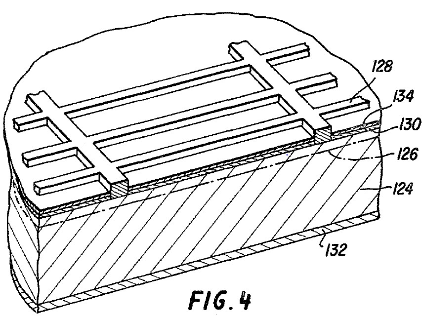
521 Nakano says at column 3 lines 28-37:
The structure of the solar cell in this embodiment is as follows:
Silicon substrate/aluminium oxide layer/tantalum pentoxide layer/(atmosphere) structure (1).
In this embodiment the thickness of the aluminum oxide coating layer is about 80 Å. Further, when it is assumed that the wavelength is 5000 Å, the refractive index of the tantalum pentoxide n is 2.2, nd is λ0/4 and d becomes about 568 Å.
522 REC Solar relies on structure 1 as so described most heavily for its arguments.
523 Nakano provides a number of variations of this structure in which additional materials are added on top of the tantalum pentoxide: structure 3 adds a silicon dioxide layer on top of the tantalum pentoxide; structure 4 adds polyvinyl butyral and glass; and structure 5 adds silicon dioxide.
524 Structure 2 is identified in Nakano as a comparative example, and includes only a silicon substrate and tantalum pentoxide, with no aluminium oxide layer.
525 A manufacturing method is then described, details of which most relevantly include the following:
4. A 5% solution of tantalum compound, mainly tantalum alcoxide (Ta(OR)4) was used, but also tantalum chelate (Ta(OH)2.(OCHRCOOH)2) or tantalum acylate (Ta(OR)3(OCOR)2) may be used, dissolved in a mixed solvent of ethanol (C2H5OH) and ethyl acetate (CH3COOC2H5), for the formation of the tantalum pentoxide thin film layer. In these molecular formulas, R represents CnH2n+1. and in this embodiment a mixture of different kinds of substances can be used, including those where the value of n is between 2 and 8.
526 REC Solar relies on the following passage located in column 8, lines 42-51, which refers to results depicted in a graph set out at figure 9. Nakano provides that the results depicted in figure 9 show the infrared absorption of a silicon wafer coated with aluminium oxide (column 8 structure):
… OH radicals are retained or trapped in the aluminum oxide coating layer, or in the interface between the aluminum oxide coating layer and the silicon wafer. In addition, 25 atom % of H was observed in the aluminum oxide layer by a nuclear reaction method. The radicals H or HO as well as their ions inactivate the surface states between the silicon and the aluminum oxide. The inactivation of the interface level prevents the carriers from being trapped by the interface and thereby decreases the velocity of recombination.
(Emphasis added.)
527 The experts agree that 25 at. % of hydrogen is a high hydrogen content that would be sufficient to achieve surface passivation, and similarly that the statement concerning the effect of the radicals H or HO and their ions discloses and states that hydrogen is passivating the surface of the substrate.
11.3.4 “hydrogen being embedded into the second dielectric layer” – integer 9(g)
528 In relation to integer 9(g), REC Solar contends that Nakano discloses the use of hydrogen-containing compounds to form the second dielectric layer, which is the tantalum pentoxide layer, and that it also discloses that both the 5% solution and the solvent to be used to form the tantalum pentoxide layer contain “a substantial amount of hydrogen”. It submits that these matters support the view that there is a sufficient amount of hydrogen present in the tantalum pentoxide layer prior to firing to satisfy the requirement in 9(g) of “hydrogen being embedded into the second dielectric layer”. In this regard, it contends that the evidence of Professor Weber that he was “fairly certain” and of Professor Weber and Professor Cuevas-Fernandez that it was “very likely” that there would be hydrogen in the tantalum pentoxide are sufficient to establish anticipation.
529 Hanwha submits first, that integer 9(g) requires hydrogen to be present in the second dielectric layer in its “as-deposited state” in a form enabling it to be released during a subsequent high-temperature firing step. Next, Hanwha submits that even if the “embedded” aspect of integer 9(g) is to be construed as requiring that hydrogen is present in the second dielectric layer, REC Solar has not proved its case. In this regard it submits that neither of Professors Weber or Cuevas-Fernandez considered it to be inevitable that there would be hydrogen in the tantalum pentoxide layer in circumstances where there is no literal disclosure of the integer and accordingly REC Solar relies on a case based on inevitable result, citing AstraZeneca FFC at [298].
530 I have in section 2.6 concluded that integer 9(g) must be understood as requiring hydrogen to be present in the second dielectric layer, irrespective of form or amount. Accordingly, Hanwha’s first argument must be rejected. The second argument concerns whether or not REC Solar has discharged its onus of establishing the presence of hydrogen. For the reasons that follow, in my view it has done so.
531 In the Validity JER Professor Cuevas-Fernandez considered that the claim required the hydrogen to be in a form that enables it to be released during a high temperature firing step, and that the form in which it is disclosed in Nakano would be unlikely to meet that requirement.
532 Professor Weber considered that the form in which the hydrogen is present is immaterial in determining whether or not hydrogen is “embedded” and that accordingly, integer 9(g) of claim 9 was disclosed.
533 Professor Weber said in his affidavit evidence:
Although Nakano does not explicitly refer to “hydrogen being embedded into the second dielectric layer” for the purpose of [integer 9(g)] of the Patent claims, based on my knowledge and experience in the field of silicon solar cells as at November 2007, I knew that the use of hydrogen-containing precursors to form a dielectric film would result in the film containing an amount of hydrogen. As set out in the Nakano Comparison Table, Nakano discloses the use of hydrogen-containing compounds to form the tantalum pentoxide layer … claim 9 [of the patent] does not require a specific amount of hydrogen to be “embedded into the second dielectric layer”.
534 When Professor Cuevas-Fernandez engaged with Professor Weber on this construction, he accepted that the part of Nakano that disclosed the solution to be used to form the tantalum pentoxide layer did disclose the use of hydrogen-containing compounds to form the tantalum pentoxide layer (as stated by Professor Weber), and also that the solvent in which the solution is to be mixed would contain a substantial amount of hydrogen. He said, however, that he was not “scientifically convinced” that the presence of hydrogen in the chemicals used for preparing the tantalum oxide “can confidently lead to the conclusion that hydrogen will be present in the final layer” because of the process by which the solar cell was made. When pressed, he accepted that it is “possible” and “maybe even likely” that hydrogen would be present.
535 In response, Professor Weber accepted that the process described in Nakano involved a heat treatment at 500 °C which would significantly diminish the amount of hydrogen present saying:
… So that will presumably result in a loss of much of the organics which will include the loss of a significant amount of the hydrogen, so I do agree that the hydrogen content following the heat treatment will be significantly reduced. I think it’s very likely that there will be some hydrogen left … I’m fairly certain that there will be hydrogen in the final compound. In terms of how much hydrogen that will be, that is a much harder question to answer.
536 The experts gave further relevant evidence as follows:
PROF WEBER: … Another interpretation would be that the reason why it’s mentioned in 9 [being claim 9 of the patent] is because if you have hydrogen present prior to firing, then some amount of hydrogen will also be present after firing even though that hydrogen no longer serves any purpose, but either way claim 9 by itself is extremely broad and it’s really far broader than the disclosure of the patent.
HIS HONOUR: Yes. So if it’s the second interpretation then it wouldn’t matter if it was the nearest [sic, merest] of trace elements of hydrogen because it’s an artefact of a previous step.
PROF WEBER: That is true to some extent, your Honour, but then I think the issue becomes again that I think even in instances where you made a solar cell where you don’t – for example, you don’t have a firing step and you don’t intentionally introduce hydrogen, almost inevitably some trace amount of hydrogen will be present anyway because hydrogen is very difficult to completely keep out of any material. It’s just ubiquitous. So it again becomes a question around how much hydrogen is required for – embedded – for it to be embedded.
HIS HONOUR: So do I understand that to mean that you might have a trace amount of hydrogen in the second layer after production and yet still not have sufficient hydrogen to assist in passivation.
PROF WEBER: That’s correct.
HIS HONOUR: Professor Cuevas, do you agree with all of that?
PROF CUEVAS-FERNANDEZ: Yes. Yes.
537 I have found in section 6.6 (construction) that this integer must be understood as requiring hydrogen to be present in the second dielectric layer, irrespective of form or amount. Accordingly, only a small amount of hydrogen will be sufficient to meet the requirement and, as Professor Weber said at the commencement of the quote above and, as Professor Cuevas-Fernandez agreed, if one has hydrogen present prior to firing, then some amount of hydrogen will also be present after firing.
538 The relevant legal question is aptly summarised in General Tire at 485-486 as follows:
The prior inventor, however, and the patentee may have approached the same device from different starting points and may for this reason, or it may be for other reasons, have so described their devices that it cannot be immediately discerned from a reading of the language which they have respectively used that they have discovered in truth the same device; but if carrying out the directions contained in the prior inventor’s publications will inevitably result in something being made or done which, if the patentee’s patent were valid, would constitute an infringement of the patentee’s claim, this circumstance demonstrates that the patentee’s claim has in fact been anticipated.
539 The experts in this case, as scientists tend generally to be, were cautious in expressing opinions in terms of absolutes. It is in this context that I regard the evidence of Professors Weber and Cuevas-Fernandez as to the general ubiquity of hydrogen and the probability that hydrogen will be present in the second dielectric layer as disclosed in the Nakano publication as sufficient to satisfy me that in carrying out the directions disclosed the second dielectric layer the skilled reader would inevitably result in something which would constitute infringement of this aspect of claim 9 of the patent.
540 Accordingly, I find that integer 9(g) is present and disclosed. This was the only disputed aspect of claim 9.
11.3.5 “surface of the silicon substrate is passivated by hydrogen” – claim 16
541 Hanwha contends that the combination represented by claim 16 when dependent on claim 9 is not disclosed in Nakano for three reasons: first, because structure 1 as disclosed in Nakano has a p-type base substrate and a diffused n+ layer at the front, which Professor Cuevas-Fernandez considered meant that it was unlikely that the surface was passivatable because the phosphorous doping at the time (the early 1980s) was “so heavy that the surface would be most likely insensitive to an attempt to passivate it”; secondly, any reliance on the column 8 structure, which is not the same as structure 1, involves impermissible mosaicking of discrete parts of Nakano; and, thirdly, in any event: (a) the passivation characteristics of structure 1 cannot be compared with the column 8 structure because Nakano does not indicate if and how the column 8 structure is doped; (b) the aluminium oxide layers on the column 8 structure are of different thicknesses to structure 1, such that the results in relation to the column 8 structure cannot be compared with structure 1; (c) the results disclosed in Nakano were considered by Professor Weber to be “questionable to some extent” because of how they were derived.
542 The first argument cannot withstand the express disclosure of Nakano at column 8, which states in terms that passivation was achieved. The relevant passage is at lines 42-51:
… OH radicals are retained or trapped in the aluminum oxide coating layer, or in the interface between the aluminum oxide coating layer and the silicon wafer. In addition, 25 atom % of H was observed in the aluminum oxide layer by a nuclear reaction method. The radicals H or HO as well as their ions inactivate the surface states between the silicon and the aluminum oxide. The inactivation of the interface level prevents the carriers from being trapped by the interface and thereby decreases the velocity of recombination.
543 In his oral evidence Professor Cuevas-Fernandez accepted that Nakano is here stating that the hydrogen is passivating the surface of the substrate and that the quantity of hydrogen reported in that passage would be sufficient to passivate the surface. That evidence accords with the plain meaning of the passage quoted.
544 The second concerns what Hanwha contends is the impermissible blurring of the disclosure in column 8 with the earlier disclosure of structure 1. It will be recalled that the column 8 passage refers to tests undertaken in relation a silicon wafer coated with aluminium oxide alone, not to a dielectric layer stack consisting of aluminium oxide and tantalum alcoxide (which is the form that structure 1 takes). Accordingly, the tests were not conducted on a dielectric layer stack conformable with the structure of claim 9.
545 REC Solar submits that it may be assumed that the results from the tests performed on the column 8 structure may be applied directly to the dielectric stack of structure 1. That is an assumption drawn from the general statement at the conclusion of Nakano at column 10 to the effect that the present invention “provides a solar cell of high performance”. REC Solar contends that this statement provides a foundation for a conclusion, as a matter of construction, that the advantages taught in relation to the column 8 structure apply equally to structure 1. That contention is supported by the expert evidence.
546 Professor Cuevas-Fernandez accepted in his oral evidence that the reason for the passage in Nakano is to teach and disclose the benefits of the composite stack layer that is subsequently claimed (which included structure 1). Although he expressed scepticism about the results as to there being surface passivation, that was based on his understanding that Nakano had used a particular concentration of phosphorous atoms in the process of doping the silicon wafer that would lead to emitters that were too heavily doped to benefit significantly from passivation. However, nowhere was the concentration of phosphorous atoms used disclosed in Nakano.
547 Furthermore, Nakano itself teaches that surface passivation was achieved, as Professor Cuevas-Fernandez accepted. That was also the evidence of Professor Weber, who considered that the results obtained using an aluminium oxide structure would be the same if a layer of tantalum pentoxide is placed on top – he expected that similar amounts of hydrogen would be present in the aluminium oxide.
548 Professor Cuevas-Fernandez also contended that as there was a difference in the thickness of the aluminium oxide layer in the column 8 structure (74 nm) and structure 1 (8 nm), he considered that this “may or may not have relevance” and he “would not expect much hydrogen left at all”.
549 Professor Weber accepted that the change in thickness is likely to reduce the amount of hydrogen, but that it would still be in the range of a few atomic percent and it was quite possible that it would remain the same. When it was put to him that there may be difficulties with extrapolating the numbers, he agreed that whilst the exact numbers given in relation to the column 8 structure could not be directly applied to structure 1, the amount of hydrogen would remain significant for structure 1.
550 I consider that Professor Cuevas-Fernandez did not in the case of Nakano confine himself to reading the disclosure of the document in the light of the common general knowledge, but applied idiosyncratic parts of his own knowledge to discount its disclosure. In my view Professor Weber took a more suitable approach to the document. Both experts agreed that the references to the column 8 structure were made for the purpose of teaching the skilled reader that surface passivation was achieved by the hydrogen, not only in relation to that structure but to the invention as described in Nakano. I prefer the evidence of Professor Weber that this was a disclosure that was applicable to structure 1, not only because that is the teaching of the document, but also because it was scientifically available.
551 Accordingly, in my view the additional integer in claim 16 is disclosed in Nakano.
11.3.6 Conclusion in relation to Nakano
552 For the reasons set out above, I conclude that claim 9 is anticipated. Hanwha accepts that such a finding leads to the result that claims 12 and 21 are also not novel. I have also concluded that claim 16 is anticipated with the result that claim 16 and claim 21 (when dependent on claim 16) are not novel.
553 REC Solar contends that Bhattacharyya anticipates claims 9 and 11 only. I have concluded above that, by reason of the disclosure of Nakano, claim 9 is anticipated.
554 It is not necessary to dwell unduly on the disclosure of Bhattacharyya. Hanwha contends that most of the integers of claim 9 are absent from it. It is sufficient for present purposes to note that at [0083] and [0084] of Bhattacharyya a first dielectric material is described to be “in direct physical contact with both semiconductor-enriched insulator 304 and second layer 208 of semiconductor material”. In their oral evidence, the experts agreed that the second layer disclosed in Bhattacharyya need not necessarily be a dielectric layer but could be a layer of semiconductor-enriched insulator which does not need to be a dielectric. Bhattacharyya accordingly does not provide clear directions to produce something within the claim. In light of that evidence, integer 9(e) is absent from the disclosure of Bhattacharyya.
555 Furthermore, in my view there is no disclosure of hydrogen being embedded into the second dielectric layer as required by claim 9 integer (g). The publication makes no reference to hydrogen and has no discussion of it at all. At [0024] of Bhattacharyya it is said that “[t]he semiconductor-enriched insulators utilized in the various aspects of the invention described herein can be formed by any suitable methodology” (emphasis added). Whilst some of the methods then identified may have included the use of hydrogen, Professor Weber accepted that one of the commonly known methodologies that could have been used to form the semiconductor enriched insulator was sputtering, which uses little hydrogen. In the absence of a disclosure of hydrogen being a required feature, and having regard to the fact that one of the suitable methodologies at the time was sputtering, I am not persuaded that this integer in claim 9 is disclosed.
556 Accordingly, Bhattacharyya does not anticipate either claim 9 or claim 11 when dependent on claim 9.
557 REC Solar contends that the alleged invention as claimed in the challenged claims is not a patentable invention for the purposes of s 18(1)(c) of the Patents Act in that those claims include solar cells containing dielectric layers that do not achieve the promise of the invention.
558 The relevant unmet promise alleged is that every solar cell falling within the scope of the challenged claims will have the following beneficial properties, produced using an economical and industrially viable method:
(1) very good surface passivation on either n- and p-type silicon surfaces; and/or
(2) very good optical properties.
559 Hanwha submits that REC Solar pitches the promises made in the specification too broadly and that the promises alleged have not been made in the specification. It further contends that in any event the evidence does not support the proposition that the alleged promises have not been met.
560 In Merck Sharp & Dohme at [432]-[441] I summarised the law in relation to lack of utility as set out below.
432 Section 18(1)(c) of the Patents Act provides that an invention is a patentable invention for the purposes of a standard patent if the invention, so far as claimed in any claim, is useful. Until recently, the requirement that an invention so far as claimed be “useful” within s 18(1)(c) was defined solely by reference to the common law development of that concept. The words in Lane Fox v Kensington and Knightsbridge Electric Lighting Co [1892] 3 Ch. 424 at 431 of Lindley LJ (with whom Lopes LJ agreed) set the scene (emphasis added):
The utility of the alleged invention depends not on whether by following the directions in the complete specification all the results now necessary for commercial success can be obtained, but on whether by such directions the effects which the patentee professed to produce could be produced, and on the practical utility of those effects.
433 What the patentee “professed to produce” is to be ascertained by having regard to what is now routinely referred to as the “promise of the invention” being the promise that the specification is said to make of the invention claimed: Rehm Pty Limited v Websters Security Systems (International) Pty Limited [1988] FCA 232; 81 ALR 79 at 84 and 96 – 97 (Gummow J); Décor Corp Pty Ltd v Dart Industries Inc [1988] FCA 682; 13 IPR 385 at 394 (per Lockhart J). This is assessed as a matter of construction of the specification: see generally ESCO Corporation v Ronneby Road Pty Ltd [2018] FCAFC 46; 358 ALR 431 at [182] – [239] (Greenwood, Rares and Moshinsky JJ).
…
436 In each case it is necessary to consider the nature of the promise of the invention by reference to the specification and also whether that promise is met by that which is the subject of the claims. Often that enquiry gives rise to a question of claim construction: if a broad claim includes something that does not meet the promise of the invention, will it be invalid for want of utility? In this context at first blush there appears to be some tension in the authorities.
437 One relevant principle of claim construction is that it is not legitimate to narrow or expand the boundaries of the monopoly as fixed by the words of a claim by adding to those words glosses drawn from other parts of the specification: see Welch Perrin at 610. In H Lundbeck A/S v Alphapharm Pty Ltd [2009] FCAFC 70; 177 FCR 151 at [81] Emmett J said that:
A claim is bad if it covers means that will not produce the desired result, even if a skilled person would know which means to avoid. That is to say, everything that is within the scope of a claim must be useful, otherwise the claim will fail for inutility (see William WM Wrigley Junior Company v Cadbury Schweppes Pty Ltd (2005) 66 IPR 298 at [138]).
438 However, that is not to say that for the purposes of the inutility ground of revocation claim construction should be approached mechanistically. The passage from WM Wrigley Jr Co v Cadbury Schweppes Pty Ltd [2005] FCA 1035; 66 IPR 298 at [90] (Heerey J) at [138] to which Emmett J referred was as follows:
A claim is bad if it covers means that will not produce the desired result even if a skilful person would know which means to avoid: Norton and Gregory Limited v Jacobs (1937) 54 RPC 271 at 276, Welch Perrin & Co Pty Limited v Worrel (1961) 106 CLR 588 at 601, Martin Engineering Co v Trison Holdings Pty Ltd (1989) 14 IPR 330 at 337. Menzies J pointed out in Welch Perrin (at 602) that this does not mean that a specification should be construed in a way that any sensible person would appreciate would lead to unworkability when by construction it could be given a more limited meaning. However, in the present case the claims read in the light of the specification as a whole distinguish between those claims which specify a particular amount of hydrogenated isomaltulose (2, 3 and 15) and the remainder, which do not. To imply a minimum of 50 per cent in the latter claims would be, in the words of Lord Greene MR in Norton (at 276) not to construe the specification but to amend it. I therefore uphold this ground.
439 From here it may be seen that the question of whether a broad claim is construed to lack utility is governed by whether a sensible person (in the art) would realise that a claimed approach would lead to unworkability, and not apply that. In Lundbeck, the relevant claim under consideration was claim 5, which provided for a pharmaceutical composition according to claim 3 or 4, with an active ingredient present in an amount from 0.1 to 100 milligrams per unit dose (at [44]). Emmett J did not find it necessary to reach a conclusion in respect of the utility argument advanced, because he found the invention claimed not to be novel. Bennett J found claim 5 to lack utility, with whom Middleton J agreed (at [218]), whilst claims 3 and 4 were found not to lack utility.
440 It is apparent that a claim will lack utility if, by its proper construction, the skilled person is compelled to make something that does not meet the promise, or otherwise fails to work. This was explained by Bennett J in Austal Ships Pty Ltd v Stena Rederi Aktiebolag [2005] FCA 805; 66 IPR 420 (bold emphasis added, italics in the original):
[235] In Welch Perrin at 602, the alleged lack of utility was that the claims were so general that an unworkable machine could be made in conformity therewith, although a most useful machine could also be made within the claim. Menzies J, at 601, considered the principle that all within the scope of the claim must be useful if the claim is not to fail for inutility. His Honour refined the principle in Norton and held that a specification should not be ‘construed in a way that any sensible person would appreciate would lead to unworkability when by construction it could be given a more limited meaning’ (at 602).
[236] It is apparent that in Washex Machinery at 18, Stephen J was of the view that the claim did not need to specify a limitation that was common knowledge in the art for that limitation to apply. Further, to postulate “a quite purposeful adoption” of a form which would obviously malfunction was “not an appropriate mode of testing validity of a patent specification”.
[237] In Martin Engineering Co v Trison Holdings Pty Ltd (1989) 14 IPR 330 at 336-338 (‘Martin Engineering’), Burchett J discussed lack of utility, both in the sense of the claims asserting a monopoly, over the useful and the non-useful and also in the failure of the range of claimed devices to fulfil the promise of the specification, to overcome the identified problem. As to the former, Burchett J accepted that if, on its correct construction a claim asserts a monopoly in respect of something useful and also in something not useful, the patent is bad. However, his Honour observed that Norton was decided on the proper construction of the claims. Burchett J distinguished the reasoning [in] Norton in cases where the words of the claim were not “clear words” (at 337 – 338). Rather than adopt Lord Greene’s concept of a rigid separation of claim and body of the specification, his Honour said that the claims are not to be construed without regard to the specification of which they form part. He also affirmed the necessity to consider the claims as would the person skilled in the art desirous of making use of the invention. This included ‘limitations dictated by common sense after a perusal of the whole of the specification including the claims’ (at 338). That approval is, in my opinion, consistent with proper claim construction in Australia.
441 In Sandvik Intellectual Property AB v Quarry Mining & Construction Equipment Pty Ltd [2017] FCAFC 138; 348 ALR 156 the Full Court (Greenwood, Rares and Moshinsky JJ) endorsed the above reasoning as correct (at [192]). The outcome of Sandvik on its facts illustrates the approach. There, the Court was concerned with claims to an extension drilling system that used extension rods and included a drive chuck for driving the outside surface of a coupling. Claims 1 – 3 included no limitation as to the means by which the rods were driven. Claim 4 was construed to require that the rods had a hexagonal or round cross-section. The primary judge had found on the evidence that a rod with a round profile would not work in a chuck. The consequence was that claim 4 was correctly found by the primary judge to lack utility (at [201] – [202]). However, claims 1 to 3 did not lack utility: even though the invention claimed in claim 4 fell within the scope of those claims, the Full Court found that the skilled addressee would not read claims 1 to 3 as including extension rods with a round end (at [203]).
12.3 The very good surface passivation argument
561 REC Solar submits that the very good surface passivation promise arises from several of the passages in the patent including that which identifies the “key to understanding the outstanding passivating effect” on page 5 lines 10-16 and the passage at page 10 lines 13-21 which relevantly provides:
In summary, the method or the solar cell according to aspects and embodiments of the present invention is distinguished from previously known methods … in terms of the following points:
(i) very good surface passivation, such as is necessary for achieving high degrees of solar cell efficiency, can be achieved even after a firing step in the temperature range of 800-900 °C;
(ii) both low and high doped n- and p- type silicon surfaces can be passivated very effectively; …
(The complete passage is set out in section 5.1.)
562 REC Solar submits that, despite the promise of very good surface passivation on either n- or p-type silicon surfaces, Professors Weber and Cuevas-Fernandez agreed that the use of lightly doped n-type surfaces would be problematic in practice due to the potential formation of a parasitic shunt and that it is necessary to qualify a claim of effective passivation that results in parasitic shunt because, even though one may achieve good passivation, in doing so one may well have the effect of reducing the efficiency of the solar cell.
563 Hanwha submits that the promise of the invention is to be understood from the paragraph immediately under the heading Summary of the Invention on pages 3-4 of the specification, where it is said that there may be a need for a solar cell in which, on the one hand, good passivation of the surface can be achieved and, on the other hand:
… the above-mentioned drawbacks of conventional surface-passivating layers can be at least partially avoided. In particular, it should be possible to produce solar cells displaying very good surface passivation in an economical, industrially viable manner.
This need can be met by the subject matter of the independent claims.
(page 4 lines 1-6)
564 The “above-mentioned drawbacks” are those described in the Background section.
565 Hanwha contends that the Patent does not promise that the dielectric layer double layer will passivate every surface equally. Nor does it promise that every embodiment within the independent claims will necessarily have very good surface passivation.
566 In my view the very good surface passivation argument cannot succeed for the following reasons.
567 First, I do not consider that the specification involves a promise that all embodiments that fall within the challenged claims will achieve very good passivation. There is a promise within the specification that by making a product in accordance with the claims the skilled reader is likely to be able to achieve very good surface passivation. However, I do not accept that the promise is that any solar cell falling within the claims will necessarily achieve very good surface passivation. The statement from page 4 quoted above provides in terms that “it should be possible” to produce solar cells displaying very good surface passivation. The passage relied upon by REC Solar on page 10 at (i) is couched in terms that very good surface passivation can be achieved and in (ii) that both low and high doped n- and p-type silicon surfaces can be passivated very effectively. The specification does not provide a promise that every embodiment falling within the claims will provide very good passivation.
568 The evidence from the experts indicates that considerable (but routine) work would be required in implementing the invention disclosed and described in the specification. The skilled worker, armed with the disclosure of the specification, would have to exercise a degree of skill to arrive at a solar cell that achieved the promise of achieving very good surface passivation. The specification does not promise that every double dielectric layer stack located on the surface of the silicon substrate within claim 9 will achieve very good surface passivation. However, with the exercise of routine skill of one in the art, it promises that very good passivation would be able to be achieved. Accordingly, I reject the submission advanced by REC Solar that the specification promises that every embodiment within claim 9 (and dependent claims) will have very good surface passivation.
569 Secondly, whilst Professors Weber and Cuevas-Fernandez agreed that the use of lightly doped n-type surfaces would be “problematic in practice”, this was due to the potential formation of a parasitic shunt which is a mechanism that serves to reduce the efficiency of the solar cell, but does not affect the surface passivation. In fact, parasitic shunting is, as they agreed, not a passivation problem at all. They explained in the Validity JER that lightly doped n-typed surfaces can be passivated very effectively using the processes and structures disclosed in the specification but that, in the rear region of a PERC cell, a lightly doped p-type structure passivated with a dielectric layer containing a positive charge (such as silicon nitride) may result in an inversion layer which is in intimate contact with the heavily p-doped region under the metal contact which was known to result in parasitic shunting that significantly lowers solar cell efficiency. However, the evidence disclosed that it is possible to create a solar cell in which the aluminium oxide layer is placed on a lightly doped n-type silicon without creating a parasitic shunt, and whether or not an inversion layer leads to the formation of such a shunt depends on the specific solar cell structure (though such solar cell structures were not industrially relevant as at 2007).
12.4 The very good optical properties argument
570 REC Solar contends that the promise that all embodiments of the invention of the challenged claims will have very good optical properties arises from the passage on page 11 at lines 1-6 of the specification which provides:
(v) it is possible to achieve in a simple manner very good optical properties of the layer system that can be adapted very easily to the requirements of the solar cell by way of the thickness and the composition of the, for example PECVD-deposited, layer, so that the layer system can for example be embodied as an antireflection layer on the front of the solar cell or as an infrared reflector on the back of the solar cell in combination with a metal coating over the entire surface of the passivating layer.
571 REC Solar submits that there is no upper limit to the thickness of the second dielectric layer in any of the challenged claims and that accordingly those claims could include a second dielectric layer of any thickness including, for example, a silicon nitride layer of 1000 nm at the front of the cell. The experts agreed that 150 nm for the front side would be an “upper limit” which would plainly not have very good optical properties.
572 In my view this ground is not established. The promise of the specification is not that every conceivable embodiment falling within the claims will have very good optical properties, but, as it says in (v), it is possible to achieve such properties. Whilst there is no upper limit on the thickness of the second dielectric layer in any of the challenged claims, there is no sensible basis in the evidence to consider that the person skilled in the art would wish to do so. Indeed, as Professor Weber offered in his oral evidence, because of the increased cost and other adverse effects, no manufacturer would contemplate using 150 nm for an anti-reflection coating at the front of the solar cell. He does not consider that such a thickness is what the patent intended.
573 REC Solar contends that the specification of the patent does not comply with the requirements of s 40(3) of the Patents Act in that claims 16, and claims 17-21 to the extent that they are dependent on claim 16, are not clear and succinct because:
(a) The phrase “wherein the surface of the silicon substrate is passivated by hydrogen” is unclear and ambiguous and there is no workable standard for determining whether that feature is present;
(b) If the phrase “hydrogen being embedded into the second dielectric layer” in claim 9 is construed so as to require a minimum concentration of hydrogen, then it is ambiguous because there is no workable standard for determining whether the feature is present.
574 Given that I have found that integer 9(g) does not require a minimum concentration of hydrogen, the argument identified in (b) may be set to one side.
575 A valid claim is required to define with sufficient certainty the scope of the monopoly being claimed. Given that a patent is a public instrument, the claim must be defined in such a way that it is not reasonably capable of being misunderstood so that others know the “exact boundaries of the area within which they will be trespassers”: Electric & Musical Industries Ltd v Lissen Ltd (1939) 56 RPC 23 at 39 per Lord Russell of Killowen. A claim will lack clarity if a person skilled in the relevant art cannot ascertain whether what he proposes to do falls within the claim’s ambit.
576 In Kauzal v Lee [1936] HCA 39; 58 CLR 670, Dixon and McTiernan JJ addressed at 685-686 a complaint that a claim was ambiguous. One aspect of the complaint was resolved by applying the normal rules of construction to the disputed integer and reaching a conclusion as to its meaning. However, that left a further complaint, which was that the claim was so vague that the scope of the monopoly was so indefinite that the claim failed. This arose from the generality of the language used in the phrase in question which, it was contended, made it difficult for the reader to understand the ambit of the claim. The Court found that the complaint was not made out because any uncertainty could be resolved having regard to the particularity of the description of other elements in the claim which enabled any confusion caused by the general language used in the disputed integer (as to the quantity of drench that was “predetermined” for drawing up by a plunger) to be resolved by having regard to the other integers of the claimed device in question as a whole. Accordingly, although the claim might have failed for ambiguity, there was sufficient information within the claim to enable it to be understood by those in the art.
577 In relation to (a), REC Solar submits that the additional integer in claim 16 that the surface of the silicon substrate is “passivated by hydrogen” provides no workable standard by which the person skilled in the art is able to determine whether a particular solar cell falls within the scope of the claim, citing the evidence of Professor Weber to the effect that it would be very difficult and complicated to determine experimentally whether the surface is passivated by hydrogen.
578 Hanwha submits that the complaint made by REC Solar is one of proof, not of comprehension, and that the claim must be understood in a practical, common-sense manner such that mere technicalities should not defeat the grant of protection, citing Flexible Steel Lacing v Beltreco [2000] FCA 890; 49 IPR 331 at [81] (Hely J). It submits that there is no ambiguity.
579 In section 6.9 I considered the phrase “wherein the surface of the silicon substrate is passivated by hydrogen” in claim 16 and noted the agreement of the experts that the claim does not require that the silicon substrate solely be passivated by hydrogen, not least because the purpose of the aluminium oxide layer is also to provide passivation.
580 I have in section 6.6 considered the phrase “hydrogen being embedded into the second dielectric layer” in the context of claim 1, integer (d) and claim 9 integer (g). I concluded that the meaning of “embedded” is to be understood as meaning “fixed or lying in a surrounding mass”. In the context of claim 9, that requires hydrogen simply to be present in the second dielectric layer. I rejected the submission that “embedded” within claim 9 contains within it a requirement that hydrogen be confined to any particular form. That construction leads to the conclusion that the alternative lack of clarity argument identified in (b) is not available.
581 The point now raised is whether or not there is a lack of clarity about the requirement added by claim 16.
582 In the context of understanding claim 16 as dependent on any of claims 9-14, the requirement that the surface of the silicon substrate is passivated by hydrogen should, as a matter of construction, be understood to add a different or additional requirement to the claim 9 requirement that it simply be present in the second dielectric layer. The question then arises: what will that requirement be?
583 The experts agreed that as at November 2007, there was no experimental evidence on surface passivation by a stack formed by an aluminium oxide layer and a second dielectric layer. Professor Weber gave the opinion in his affidavit evidence that claim 16 provides no threshold for the level of hydrogen passivation at the surface of the silicon substrate that is required and that it would be “very difficult and complicated to determine experimentally whether the surface of the silicon substrate is passivated by hydrogen”. Professor Cuevas-Fernandez gave evidence that even if no firing step is used during the manufacture of the solar cell, some hydrogen diffusion to the silicon surface from the second dielectric layer might occur during other manufacturing steps.
584 It is apparent that the mere presence of hydrogen at the surface of the silicon substrate will not be sufficient to meet the requirement of the claim, otherwise claim 16 would be redundant when read with claim 9. However, the claim in terms provides a metric for determining infringement, namely that where there is such hydrogen at the surface of the silicon substrate as will lead to passivation (wherein hydrogen atoms donate electrons to fill dangling bonds) the claim will be satisfied. The provision of that metric is sufficient to lead to the conclusion that the clarity challenge to claim 16 (and dependent claims) cannot succeed. The argument advanced by REC Solar is that the person skilled in the art cannot know whether or not they infringe because it is difficult to determine whether the surface of the silicon substrate has been passivated by hydrogen. However, it was known at the time by those in the art that a hydrogen atom is able to passivate the surface of a silicon substrate by donating electrons to fill dangling bonds at that surface. The additional requirement of claim 16 is that some such electrons are donated. It may be that this is difficult to test, but there is no absence of clarity as to the requirement of the claim: the result is achieved if (to any degree) the hydrogen atoms donate electrons to fill dangling bonds in the silicon surface.
585 REC Solar contends that in letters and media releases issued before the commencement of these proceedings Hanwha Solutions made assertions that each of the REC Solar parties (being the cross claimants) had infringed claims patent. They contend that as a result of a finding that REC Solar does not infringe the claims it necessarily follows that Hanwha Solutions has made unjustified threats of patent infringement in contravention of s 128 of the Patents Act.
586 Hanwha accepts that the letters of demand that it sent prior to the proceedings involved threats of patent infringement and that the consequence of my finding that REC Solar does not infringe any claim of the patent will be that those threats are unlawful. However, it disputes that the media releases constitute threats within the terms of s 128.
587 Section 128 of the Patents Act provides:
Application for relief from unjustified threats
(1) Where a person, by means of circulars, advertisements or otherwise, threatens a person with infringement proceedings, or other similar proceedings, a person aggrieved may apply to a prescribed court, or to another court having jurisdiction to hear and determine the application, for:
(a) a declaration that the threats are unjustifiable; and
(b) an injunction against the continuance of the threats; and
(c) the recovery of any damages sustained by the applicant as a result of the threats.
(1A) The court may include an additional amount in an assessment of damages sustained by the applicant as a result of the unjustifiable threats, if the court considers it appropriate to do so having regard to:
(a) the flagrancy of the threats; and
(b) the need to deter similar threats; and
(c) the conduct of the person who made the threats, being conduct that occurred after the person made the threats; and
(d) any benefit shown to have accrued to the person who made the threats because of the threats; and
(e) all other relevant matters.
(2) Subsection (1) applies whether or not the person who made the threats is entitled to, or interested in, the patent or a patent application.
588 In evidence is a three-page media release dated 25 March 2019 entitled “Hanwha Q CELLS files patent infringement complaint with the Federal Court of Australia against REC Group and two distributors, Sol Distribution, and BayWa r.e. Solar Systems”.
589 The media release relevantly provides:
SYDNEY, Australia, 25 March, 2019 – Hanwha Q CELLS Australia Pty. Ltd., together with Hanwha Q CELLS & Advanced Materials Corp. (collectively, “Hanwha Q CELLS”), today announced it has filed a patent infringement complaint with the Federal Court of Australia against REC Solar Pte. Ltd. (“REC”), a part of the European headquartered REC Group. This follows Hanwha Q CELLS’s commencement of patent infringement proceedings in Australia against JinkoSolar Australia Holdings Co. Pty. Ltd. and LONGi Green Technology Co. Ltd. on 12 March, 2019.
Hanwha Q CELLS also announced that its complaint against REC also names Sol Distribution Pty. Ltd. and BayWa r.e. Solar Systems Pty. Ltd. for distributing REC products in Australia that infringe Hanwha Q CELLS’s patented technology.
The Federal Court complaint alleges that REC, Sol Distribution Pty. Ltd., and BayWa r.e. Solar Systems Pty. Ltd. are importing and selling solar modules that incorporate Hanwha Q CELLS’s patented passivation technology and infringe Hanwha Q CELLS’s Australian patent rights. Hanwha Q CELLS seeks an order to stop the three companies from importing, marketing, and selling products that infringe Hanwha Q CELLS’s asserted Australian patent. Hanwha Q CELLS has made significant investments in the commercialization of the relevant technology and, as the patent owner, has the exclusive right to sell solar modules in Australia incorporating this technology.
“We do not tolerate the infringement of our intellectual property rights and we will vigorously defend our technology from being unfairly used”, said Hee Cheul (Charles) Kim, Chief Executive Officer of Hanwha Q CELLS & Advanced Materials Corp. “We commenced legal action in Australia against two distributors as we are concerned they are distributing products supplied by REC Group that incorporate our patented passivation technology…”
590 The question is whether the language (or, more broadly, the conduct) the subject of the complaint would convey to any reasonable person that the author intended to bring proceedings for infringement against the person said to be threatened; U & I Global Trading (Australia) Pty Ltd v Tasman-Warajay Pty Ltd [1995] FCA 794; 60 FCR 26 at 31 (Cooper J); Lido Manufacturing Co Pty Ltd v Meyers & Leslie Pty Ltd (1964) 5 FLR 443 at 450-451; GM Global Technology Operations LLC v S.S.S. Auto Parts Pty Ltd [2019] FCA 97; 371 ALR 1 at [532]; TCT Group Pty Ltd v Polaris IP Pty Ltd [2022] FCA 1493; 170 IPR 313 at [379]-[394].
591 It is difficult to see how the media release could amount to a wrongful threat in circumstances where it was released after the commencement of the proceedings, and reported that fact. REC Solar does not plead that the threat was made to third parties, the alleged misconduct only being that it was wrongful for Hanwha Solutions to threaten the cross claimants, who are parties to the claim. On the basis of these matters, in my view the media release does not amount to an unjustified threat that Hanwha Solutions intended to bring proceedings for infringement against the person said to be threatened. It reports that it has brought legal proceedings for infringement in accordance with the process contemplated by the Patents Act.
592 Accordingly, the claim under s 128 of the Patents Act is established only in relation to the letters of demand sent by Hanwha Solutions to REC Solar.
593 I have found that:
(a) the REC Solar products do not infringe any of the asserted claims;
(b) the ACL case advanced by Hanwha fails because its infringement case failed;
(c) REC Solar has not established that the invention claimed in any of the challenged claims lacks an inventive step;
(d) the novelty challenge advanced by REC Solar based on Isaka and Bhattacharyya fails but succeeds where it is based on Nakano, with the consequence that claims 9, 12, 16 and 21 are invalid for want of novelty;
(e) REC Solar has not established that any of the challenged claims lack fair basis, utility or clarity;
(f) the letters before action sent by Hanwha to REC Solar amount to unjustified threats, but the media release published after proceedings were commenced does not.
594 In the result, I have found that the infringement case fails and that claims 9, 12, 16 and 21 are invalid for lack of novelty.
595 I will make directions requiring the parties to confer and supply to my chambers draft orders giving effect to these reasons and proposing a timetable for further steps in the conduct of the proceedings. It is likely that the parties will be unable to agree on the question of costs. If that is so, my preliminary view is that Hanwha should pay the costs of the proceedings with the exception of the costs of the inventive step challenge, with costs to be assessed in a lump sum amount by a Registrar of the Court. However, if any party wishes to contend for a different outcome on costs, or there is dispute as to the form of Orders arising from this judgment, provision should be made in the timetable for submissions to be exchanged and the parties should give an indication whether they wish to be heard, or whether the question of costs and any other matters of disagreement as to the form of the orders can be determined on the papers.
I certify that the preceding five hundred and ninety-five (595) numbered paragraphs are a true copy of the Reasons for Judgment of the Honourable Justice Burley. |
Associate:
1. Principles of silicon solar cell operation – the photovoltaic effect
(1) Solar cells (also known as photovoltaic cells) are defined functionally as devices designed to convert light into electricity. They do this by exploiting the photovoltaic effect. The basic principles of the photovoltaic effect below as it relates to silicon are summarised below.
(2) Sunlight is composed of photons, each of which is a bundle (or “quantum”) of electromagnetic radiation. Each photon possesses a particular amount of energy, typically measured in electronvolts (eV). The energy of a photon is related to the frequency and the wavelength of electromagnetic radiation of the photon. For example, green light has a wavelength of 565-500 nanometres (nm), and photon energies of between approximately 2.19-2.48 eV. The shorter the wavelength, the higher the frequency and the higher the photon energy.
(3) Silicon is composed of silicon atoms. Each silicon atom has 14 negatively charged electrons, with two electrons in the first electron shell, eight electrons in the second shell and four electrons in the third, outermost shell. The electrons in the outermost electron shell are known as valence electrons.
(4) Crystalline silicon is composed of silicon atoms arranged in a lattice structure, with each silicon atom sharing electron pairs with four other silicon atoms. The sharing of electron pairs between atoms is known as a covalent bond. The electrons that are shared in covalent bonds in crystalline silicon are valence electrons. The lattice structure of crystalline silicon is illustrated in Figure 1 below.
Figure 1: Lattice structure of silicon.
(5) The energy levels of the electrons present in the valence shell of silicon atoms in the crystalline silicon lattice structure are referred to as the valence band (EV).
(6) At low temperatures and in the absence of light, pure silicon acts as an insulator, that is, there is almost no flow of electrons (“electric current”) through the material. However, when light containing photons of sufficient energy shines on the silicon, those photons can excite the valence electrons in silicon atoms from the valence energy band into a higher energy state, known as the conduction band (EC). Electrons having such a higher energy state in the conduction band are free to move within the silicon lattice and, since they possess a negative charge, they can contribute to the electrical conductivity of the material. When an electron moves away from the silicon atom, more precisely, from the covalent bond that has been “broken” by a photon, it leaves behind a hole in the region of the silicon lattice where it once was. Since the relevant silicon atom, which still has 14 positive charges (protons), is now surrounded by only 13 electrons rather than its usual 14, there is a net positive charge associated with the hole. Holes can also effectively move within the silicon lattice because a second electron from a neighbouring atom can “jump” into the hole, leaving now another hole where the second electron was. As a result, holes move within the lattice as if they have a positive charge. Figure 2(a) below represents the covalent bonds in a silicon crystal lattice, in circumstances where one of the electrons in a bond becomes free and an electron from a neighbouring bond moves into the “hole” that is left behind. Figure 2(b) below is a schematic representation of the energy bands in a solid, such as silicon.
Figure 2(a): Schematic representation of covalent bonds in a silicon crystal lattice
Figure 2(b): Schematic diagram showing the creation of an electron-hole pair, with the electron moving to the upper conduction band, and the hole remaining in the lower energy band, when silicon is struck by a photon (hf).
(7) Electrons and holes are therefore both charge carriers. The movement of these charge carriers in a solar cell constitutes an electric current.
2. Relevant properties of silicon for solar cells
(8) Silicon had been the material of choice for solar cells for several decades before November 2007.
2.1 Electronic properties: semiconductor features and the band gap
(9) Silicon is a semiconductor. Semiconductors can be characterised by reference to the energy gap between their valence and conduction bands (EG). This is referred to as the band gap and is the minimum amount of energy necessary to excite an electron from the valence band to the conduction band.
(10) Insulators have a large band gap, such that, at room temperature, few electrons from the valence band have sufficient energy to jump the band gap to reach the conduction band. In comparison, conductors have no band gap between the valence and conduction bands, such that these bands merge into a single band. This means that there is no impediment for them to move to a slightly higher energy level, for example by gaining the kinetic energy associated with their movement. Therefore, in conductors, the outer shell electrons can move freely and conduct electricity.
(11) Semiconductors like silicon have band gaps that are greater in size than that of a conductor but narrower than that of an insulator. At room temperature, some electrons in a semiconductor will have sufficient energy to move from the valence to the conduction band. However, semiconductors are sensitive to temperature, such that the number of electrons with sufficient energy to move from the valence to the conduction band increases as the temperature increases.
(12) In the case of silicon, the band gap is approximately 1.1 eV. In general, photons which have less energy than the band gap energy will pass through the silicon, such that the energy from those photons cannot be exploited by the semiconductor material. Photons having an energy equal to or greater than the band gap energy (ie equal to or greater than 1.1 eV) will be able to excite electrons in the valence band to jump to the conduction band, creating an electron-hole pair. Where photons have substantially more energy than the band gap energy, the additional energy will be lost as heat. There is thus an optimum band gap that captures the maximum amount of energy from the sun possible without excessive energy loss.
(13) In an effective solar cell, solar energy must be converted into electrical energy. This means the solar cells must be designed to impart the energy from the photons to charge carriers (electrons or holes) and be able to extract that energy from the carriers. In materials such as metals, when the solar energy is absorbed, it is quickly turned into thermal energy and therefore effectively lost for the purposes of power extraction. However, in a semiconductor, it is possible to retain at least some of the photon energy for a period of sufficient length to allow it to be extracted.
(14) In a semiconductor, electrons and holes that have been created by photons can recombine, in which case the energy is lost as heat. This process is referred to as recombination and is discussed further below. However, in material with a low density of recombination active defects (that may include metallic impurities, structural defects or combinations of the two), the recombination process can be sufficiently slow that at least some of the charge carriers can be extracted before recombination takes place.
2.2 Alteration of the balance of charge carriers: doping and pn junctions
(15) An advantageous property of silicon for use in solar cells is that the balance of charge carriers within the silicon wafer can be altered. Solar cells rely upon regions of imbalance between electrons and holes in order to allow the flow of an electric current and the development of a voltage. In particular, solar cells feature regions where the hole concentration is greater than the electron concentration and other regions where the electron concentration is greater than the hole concentration.
(16) Pure silicon does not have a large imbalance in the concentrations of carriers. In order to alter the balance of electrons and holes in silicon, the silicon can be doped with atoms of another element, known as a dopant. Doping involves the addition of small quantities (typically less than one part per million) of an element (the dopant) to a semiconductor in order to change its electrical properties by creating an excess of either electrons or holes (depending on the dopant).
(17) There are two types of dopants used in silicon solar cells, which are represented in Figure 3 below:
(a) P-type: These are dopants that increase the number of holes relative to the number of electrons. P-type dopants typically have three valence electrons compared to silicon's four valence electrons. These dopants are also known as “Group III” dopants as they are located in Group III of the Periodic Table. The most common p-type dopant is boron. When silicon is doped with boron, an atom of boron can replace a silicon atom in the lattice structure. The boron atom, having only three valence electrons, can accept an electron from a silicon atom, thereby forming an excess of holes (compared to electrons) in the silicon lattice (p-type silicon).
(b) N-type. These are dopants that increase the number of electrons in silicon, relative to the number of holes. N-type dopants typically have five valence electrons compared to silicon's four valence electrons. These dopants are also known as “Group V” dopants as they are located in Group V of the Periodic Table. The most common n-type dopant is phosphorus. When silicon is doped with phosphorus, a phosphorus atom can replace an atom of silicon in the lattice. This means that an extra valence electron is introduced into the lattice. The energy required to free the extra electron is much less than the band gap energy of silicon. This produces an excess of electrons (in comparison to holes) (n-type silicon).
Figure 3: Schematic of a silicon crystal lattice doped to produce n-type and p-type semiconductor material.
(18) Importantly, the product of electron and hole concentrations in crystalline silicon remains constant when the material is doped. In silicon at room temperature, the product of electron and hole concentrations is roughly equal to 1020 cm- 6 (that is, 1020 per (divided by) cm6). This means, for example, that if silicon is doped p-type, so that the hole concentration is 1018 cm-3, the electron concentration would be roughly 100 cm-3.
(19) P-type and n-type semiconductor material or regions can be joined together, or co-located, to form a pn junction. When p-type and n-type material are located beside each other, a concentration gradient exists between the two sides of the pn junction. In the dark, there will be a gradient with a decreasing concentration of holes from the p-type side to the n-type side. This is illustrated in Figure 4 below:
Figure 4: Formation of a pn junction.
(20) The concentration gradients tend to produce a diffusion of electrons and holes. As soon as holes move from the p-type side to the n-type side, and electrons move from the n-type side to the p-type side, they leave behind fixed charges (corresponding to the ionised dopant atoms) which create an electric field. This electric field exerts a force on the electrons and holes that tends to produce a drift current. The drift and diffusion forces oppose each other and the electrons and holes will eventually rearrange themselves so that, once equilibrium is reached, the profiles of the electron and hole concentrations in the dark in the region of the junction will be such that the diffusion and drift forces exactly cancel each other at every point of the junction along the profile. There is therefore no net current flow of either electrons or holes.
(21) A pn junction in a silicon solar cell was as at November 2007 commonly formed by:
(a) obtaining a silicon wafer doped with a p-type dopant. The dopant was typically added to molten silicon when growing the silicon ingot from which the wafer was obtained;
(b) heating the wafer in a furnace;
(c) introducing various gases into the furnace. For example, for a silicon wafer doped with boron (p-type bulk), phosphorus oxychloride gas is commonly used. This results in the deposition of a phosphorus-containing glass-like layer on the surface of the silicon wafer. This layer acts as a source of phosphorus atoms that are then driven into the wafer; and
(d) cooling the wafer and removing the surface layer formed by the introduction of gases into the furnace, leaving a thin, diffused region close to the surface of the silicon wafer that includes dopant of an opposite type to that present in the bulk of the wafer.
(22) The diffused region of a solar cell is commonly referred to as the “emitter”. The level of doping in the emitter region is always greater than the level of doping in the body of the silicon wafer. There are multiple considerations that determine the level of doping of a diffused region in a silicon solar cell. A lighter diffusion will generally allow better passivation and better voltage. However, it also results in lower conductivity, which results in greater power losses associated with the flow of current to the metal fingers (contacts) and further results in greater power losses associated with current flow from the diffused region into the metal contacts. In addition, both the doping level (in both the emitter and in the bulk of the wafer) and the diffusion profile (that is, how dopant concentration changes with depth) can have significant impacts on the optimum design of other aspects of the solar cell. As at November 2007, the optimum level of doping (both in the emitter and in the bulk) and diffusion profile was, and had been for many years, an important area of research.
(23) The pn junction in conventional, commercially available solar cells was as at November 2007 located in the near-surface region of the silicon facing the sun. This is because most carriers (electrons and holes) are typically generated in the region of the silicon that is closest to sunlight. The rate of sunlight absorption decreases the further light travels into the silicon wafer. The further the carriers have to travel through the silicon before they reach the pn junction, the greater the chance that they will recombine before they reach the pn junction. As more carriers are generated closer to the surface facing the sun, the pn junction is placed in that region to decrease the distance between the formation of the carriers and the pn junction and to allow for more efficient carrier collection.
(24) As at November 2007, most commercially produced silicon solar cells were made from p-type silicon. Two reasons for this were:
(a) Firstly, the use of a p-type wafer allows the pn junction to be formed by diffusing an n-type dopant such as phosphorus rather than a p-type dopant such as boron. It was (and generally remains) easier to create an n-type phosphorus-diffused region (emitter) at the front of the cell with uniform doping across each cell and with minimal defect generation in the silicon substrate, than creating a p-type boron-diffused region (emitter) of similar quality. Phosphorus diffusions also have a beneficial effect of gettering (capturing and neutralising) metallic impurities that may be present in the silicon wafer.
(b) Secondly, the use of a p-type wafer meant that the rear surface of the silicon wafer would be a “p-contact” for which aluminium (also a p-dopant) could be used. This resulted in a heavy p-type surface at the rear of the cell, with a diffused n-type region (emitter) created at the front of the cell. This arrangement was less complicated than that required for an n-type wafer, which would ideally require a heavily doped n-type region at the rear and hence a second dopant (phosphorus) diffusion.
(25) In addition, silicon nitride could be effectively used to passivate n-type emitters but was not as effective at passivating p-type emitters. It was generally well known by Skilled Persons in the Field at that time that this is due to the fact that silicon nitride contains a positive charge, the density of which can vary depending on the deposition and post-deposition processing conditions of the silicon nitride.
(26) As at November 2007, it was well-known by Skilled Persons in the Field, that there were a number of disadvantages associated with using a silicon wafer with a p-type bulk. A significant disadvantage is that the use of boron for p-type doping can result in defects in the silicon. For example, single crystal silicon grown by the Czochralski method (the most commonly used method for producing commercial single crystal silicon wafers for the photovoltaics industry) has a relatively high concentration of oxygen. On the other hand, multicrystalline silicon, produced by cast or directional solidification methods, and becoming by 2007 prevalent in industry, has a lower concentration of oxygen. Boron can form boron-oxygen defects with the oxygen in the silicon wafer that reduce the efficiency of the solar cell. Boron-doped silicon can also be negatively affected by iron, particularly in interstitial form, and other metals that may be present in the silicon wafer (as an impurity) as a result of the silicon wafer manufacturing process. Techniques such as gettering, which is described in paragraph 44 below, can be (and were as at November 2007) used to address the presence of impurities such as iron and mitigate their negative impact. These types of defects are not created to the same extent when silicon with an n-type bulk is used, although n-type silicon is not entirely free of defects.
(27) As at November 2007, there was research being conducted on the use of n-type silicon, although n-type silicon was not at that time being used to any significant extent in industry. This research included understanding the impact of different impurities on the material, as well as research on solar cell architectures based on n-type silicon, and research on passivating materials for p-type emitters for use with n-type silicon wafers.
2.3 Function of the pn junction in the operation of silicon solar cells
(28) The purpose of a solar cell is to generate power. Power is the product of current (I) and voltage (V). Therefore, in operation, a solar cell must generate both a current and a voltage such that the product of current and voltage are maximised.
(29) As discussed above, some of the photons from sunlight that are incident on the solar cell will be absorbed by the cell and generate additional electrons and holes. The electrons and holes generated by light in this way are referred to as excess carriers. Each photon can generate one electron-hole pair. In order to generate a current, electrons need to be collected by the n-type contact and holes need to be collected by the p-type contact. The pn junction facilitates the collection of carriers. For example, it was generally believed that electrons generated in the p-type region of the cell will experience an electrical field that will push them to the n-type region if they are in the region of the pn junction.
(30) The voltage of the solar cell depends on the concentration of excess carriers. Specifically, it depends on the ratio of the product of the electron and hole concentration under light to the electron and hole concentration in the dark.
(31) Excess carriers therefore need to be present in the solar cell in order for it to operate. However, these excess carriers can recombine via a number of mechanisms. Some of these mechanisms are unavoidable, and therefore impose an upper limit on the efficiency of the cell. However, some mechanisms are avoidable and therefore steps can be taken to minimise these.
(32) Silicon in the form of a polished silicon wafer is very reflective. In addition, it is a weak absorber of any sunlight that has an energy close to the silicon band gap.
(33) A number of methods can be employed in a silicon solar cell to reduce optical losses and optimise useful light absorption within the device, as set out in paragraphs 34 to 39 below.
(34) An antireflection coating (ARC) is typically employed on the side of a silicon solar cell that faces the sun. In this context, the refractive index is an important optical property of a material. The refractive index determines how light is reflected, refracted and absorbed in a material.
(35) Solar cells are encapsulated to form solar modules. The encapsulant material is located on top of the sun-facing side of the solar cells. The refractive index of the encapsulant material is typically around 1.4-1.5.
(36) Silicon in a solar cell that is not covered with any antireflection coating can be highly reflective because there is a large difference in the refractive index of silicon (around 3.9) and that of the encapsulant material. One way to reduce this reflection loss is to deposit or create on the silicon wafer a material with a refractive index intermediate between that of silicon and the encapsulant material, and of a thickness that minimises the light reflected from that surface. The optimal refractive index of the material (or materials, if more than one) used, and the optimal thickness of that material (or materials), are related.
(37) As at November 2007, silicon nitride was the material that was most commonly used to provide an antireflection coating, both in research and in industry. The refractive index of silicon nitride films deposited using commercially used methods (e.g. PECVD) varies between about 1.9-2.5. A refractive index of 2 is close to being the ideal value for providing a good antireflection coating, while minimising absorption losses, in a silicon solar cell that has been encapsulated into a solar module. As the refractive index of silicon nitride rises above 2, the silicon nitride starts to absorb a small but not insignificant amount of light, particularly in the blue part of the spectrum. For this reason, it is often desirable to use a refractive index that is a little lower than would be used purely on the basis of the reflection losses incurred.
(38) Surface texturing can be used to reduce reflection losses. This involves roughening the surface of the silicon wafer to increase the chances of reflected light bouncing back onto the surface rather than into the surrounding air. In single crystalline wafers, texturing often involves forming very small pyramids on the surface of the wafer. This is typically done on both the front and the rear of a silicon wafer. The pyramid structures that were used commercially as at November 2007 were random upright pyramids (random upright pyramids are still used commercially today). In multicrystalline wafers, different texturing techniques were used, which did not produce pyramids but other surface features that helped to reduce reflection.
(39) A back surface reflector is generally employed on the surface of the silicon wafer opposite to the sun-facing surface. When sunlight hits a silicon solar cell, not all of the light will be absorbed after one pass through the silicon. A reflector is therefore used on the back surface of the silicon wafer to make it difficult for the light to escape from the silicon. This increases the pathlength of the rays of light within the silicon to provide the light with the greatest opportunity to be absorbed. In addition, texturing of the surface of the silicon wafer opposite to the back surface reflector, reduces the likelihood that light that was reflected from the rear of the cell can escape out the front surface. Instead, most of the light will be trapped within the silicon wafer and will eventually be absorbed. It is desirable that the back surface reflector has a high reflectivity, and this can be achieved, for example, by inserting a material with a low refractive index, such as silicon dioxide, between the silicon and an appropriate metal, such as silver or aluminium.
2.4.1 Defects and Recombination
(40) Another disadvantage of silicon is that it is a sensitive material, in the sense that a low concentration of defects can severely degrade the carrier lifetime and therefore the usefulness of the silicon in a solar cell. A defect can be located within the bulk of the silicon wafer, for example, an impurity (such as a metallic impurity) or a change in the structural integrity of the crystal lattice, which can provide a pathway for electrons and holes to recombine. Defects can also be located at the surface of a silicon wafer, where there is disruption in the crystal lattice. For example, silicon atoms will exist at the surface of a silicon wafer that do not have a bonding partner. This results in an unpaired valence electron referred to as a dangling bond. Figure 5 below provides a schematic diagram of dangling bonds at the bare surface of a semiconductor.
Figure 5: Schematic diagram of dangling bonds at a bare semiconductor surface.
(41) The presence of unwanted defects in silicon results in an increase in recombination, and consequently a reduction in the lifetime of charge carriers. This increased recombination can decrease the efficiency of a solar cell.
(42) Excess carriers need to be present in the solar cell in order for it to operate. However, excess carriers can recombine through defects in the material. Therefore, minimising these defects is important to maximise the efficiency of the cell. An important metric is the excess carrier lifetime (also sometimes referred to as minority carrier lifetime), which is an indication of how long the average photo-generated carrier will remain in the material before it recombines. Reducing the number of defects in the material, increases the excess carrier lifetime. A higher excess carrier lifetime can improve both the current and the voltage in the cell and therefore improves the efficiency of the cell.
(43) Manufacturing techniques have been developed in order to reduce recombination events, including by removing defects from the silicon. These techniques include methods to reduce defects in the bulk of the silicon, for example by reducing the concentration of impurities introduced by the crystal growth or cell fabrication processes, and methods to either reduce defects at the surface of the silicon wafer or to render the defects less harmful in terms of their impact on the recombination of the excess carriers.
(44) At November 2007, one of the most important techniques to reduce impurities in the bulk of the silicon was gettering. Gettering involves diffusing additional elements into the silicon in order to neutralise or remove defects. For example, phosphorus gettering involves diffusing phosphorus, which can be done at the same time as diffusion to create the pn junction. Gettering was an active area of research for a number of years, and was especially significant at November 2007 since it meant that industrial solar cells could be manufactured using lower-quality silicon wafers, which reduced cost. It also meant that the requirements for cleanliness in solar cell manufacturing could be relaxed, at least during the early stages of its industrial development.
2.5 Techniques for reducing recombination
(45) Techniques that reduce the rate of recombination of excess carriers at the surface of the silicon, including by reducing defects at the surface of the silicon wafer, are referred to as surface passivation techniques. Surface passivation techniques that were generally well known and in industrial use as at November 2007 include chemical passivation and electronic passivation.
(46) Chemical passivation reduces the density of recombination active defects (such as dangling bonds) on the surface of a silicon wafer (chemical passivation can also occur in the bulk of a silicon wafer, most commonly by diffusion of hydrogen). Different defects will have different recombination properties, and some defects may not contribute significantly to recombination.
(47) Chemical passivation can be achieved by the deposition or growth of a passivating film (or layer) on the surface of the silicon wafer. It involves the formation of bonds between the silicon atoms at the silicon surface and other atoms that are part of the overlying passivating film (or layer) that is deposited onto the silicon surface. For example, when the overlying passivating layer (or film) is a hydrogenated silicon nitride film, all three of the constituent atoms of the hydrogenated silicon nitride, being silicon, nitrogen and hydrogen, can bond to silicon atoms at the surface of the silicon wafer to reduce the density of recombination active defects.
(48) Electronic passivation reduces the surface concentration of one carrier and therefore reduces recombination events. Because each recombination event requires one electron and one hole, when the concentration of one type of carrier is reduced to very low levels, the recombination rate is also reduced. Electronic passivation may be achieved by:
(a) the presence of charge in the overlying insulator layer (or film). This is referred to as field effect passivation because the charge in the insulator film creates an electric field at the silicon surface which attracts a particular type of carrier to the surface and results in a high concentration of either electrons or holes. For example, silicon nitride has a net positive charge that will attract negatively charged electrons to the silicon surface, thereby increasing the concentration of electrons in the surface region and decreasing the concentration of holes.
(b) heavily doping the near-surface region of the silicon (for example, by diffusing a suitable dopant into the silicon bulk). By way of example, the rear of common industrial solar cells as at November 2007 was heavily p-doped, which was done using an aluminium rear contact. Such aluminium doped region, the so-called back-surface-field region (BSF), had the function of reducing recombination at the rear surface of the silicon solar cell by reducing the concentration of electrons there. It is important to note that heavily doped regions usually come with some recombination losses themselves and are, therefore, limited in the level of surface passivation that they can provide. A good example is the p+ aluminium doped BSF region, which was identified as one of the main limitations to the performance of silicon solar cells.
2.6 Passivating dielectric layer layers in silicon solar cells
(49) The passivating layers most commonly used as at November 2007 were thermally grown silicon oxide and silicon nitride deposited by PECVD (plasma enhanced chemical vapour deposition). Both silicon oxide and silicon nitride layers are dielectric layers in solar cells.
(50) A dielectric is an electrical insulator (poor conductor of electric current) that can be polarised in an electric field. That is, when an electric field is applied to the dielectric material, the atoms or molecules within that material reorientate themselves in the electric field to produce a dipole. A dipole is a molecule that has zero net charge but that has positively and negatively charged regions within it.
(51) Another dielectric material that was being used in research as a passivating layer prior to November 2007 was silicon carbide, although this had not been used in industry.
(52) As at November 2007, amorphous silicon was being used as a passivation layer, although in the context of industrially-produced cells it had only been used in specialised heterojunction solar cells (these are described in paragraph 70(b) below). Amorphous silicon is not a dielectric material.
(53) The most commonly used passivation layers as at November 2007, silicon oxide and silicon nitride, are discussed in turn below.
2.6.1 Thermally grown silicon oxide
(54) Thermally grown silicon oxide can provide a good passivation layer as it tends to leave behind a low concentration of defects at the interface with the silicon substrate, thereby providing good chemical passivation. Thermally grown silicon oxide does not hold much charge and so does not provide much electronic passivation. Despite this, thermally grown silicon oxide films were generally regarded as being able to provide very good surface passivation, particularly when complemented with a hydrogenation step. Silicon oxide does not have ideal optical properties when applied to the sun-facing side of an encapsulated solar cell due to its low refractive index of about 1.45, which is very similar to the refractive index of the encapsulant material, and so it is preferable to put an antireflection coating on it when it is used at the sun-facing side of a solar cell in a solar module.
(55) Thermally grown silicon oxide had been used extensively in research. However, as at November 2007, it was not generally known to be used in industrially-produced solar cells.
(56) By the early 2000s, it was known to Skilled Persons in the Field, that silicon nitride deposited using PECVD could provide both excellent surface passivation and a good antireflection coating. As at November 2007, PECVD silicon nitride was commonly used in solar cell fabrication in industry and in research. As at November 2007 it was generally well-known to Skilled Persons in the Field, that silicon nitride provides surface passivation through two different mechanisms, as follows:
(a) silicon nitride is a dielectric layer which has a positive charge and therefore can provide electronic passivation when deposited on a surface of a silicon substrate; and
(b) silicon nitride deposited using PECVD also has a high concentration of hydrogen atoms (although the specific concentrations varied) incorporated into the silicon nitride film (either bonded to silicon or nitrogen atoms) as a result of the precursor gases used during the PECVD process (which is discussed below). During the manufacture of an industrial solar cell, a firing step is typically undertaken after the deposition of any silicon nitride layer to produce metal contacts. As a result of the temperature applied during that firing step (which is typically ramped up to a maximum temperature of approximately 750-850°C), hydrogen contained in the silicon nitride film becomes mobile and can diffuse from the silicon nitride layer and move in different directions. Some of the hydrogen will diffuse out of the silicon nitride layer into the atmosphere and some will also diffuse to the silicon substrate where it can passivate defects at the silicon surface (such as dangling bonds) and in the silicon bulk.
(57) Silicon nitride also has beneficial optical properties in that it is antireflective in an encapsulated solar cell, as discussed in paragraph 37 above.
(58) As at November 2007, amorphous silicon could be used as a passivation layer. Its use was mainly confined to non-diffused heterojunction solar cells, although it had been referred to in some research papers as having the potential for broader use as a passivating layer.
2.7 Methods used to deposit passivation layers
2.7.2 Thermal growth of silicon oxide
(59) Thermal growth of silicon oxide is conducted at a temperature of about 700°C or above. Generally, the oxidation temperature will be determined to a large extent by the desired oxide thickness, with a thicker oxide requiring a higher oxidation temperature and/or time, or a different process (such as the use of water vapour).
2.7.2 PECVD deposition of silicon nitride
(60) Plasma-enhanced chemical vapour deposition (PECVD) was being used in both industry and in laboratory research as at November 2007.
(61) There are two different types of PECVD used to produce silicon nitride layers for solar cells:
(a) Direct PECVD involves introducing gases (the “chemical vapour”) containing silicon and nitrogen into a chamber. For example, the gases may be silane (SiH4) and ammonia (NH3). The gases introduced into the chamber are known as precursors. The silicon substrate is also placed in the chamber at a temperature of around 400°C. Plasma (ionised gas) is generated in the chamber to assist in the reaction between the gases and the substrate. The plasma radicalises the molecules of the gases to make them charged molecules and hence more reactive. This allows for a silicon nitride film to be formed more rapidly than it would form in the absence of the plasma. The plasma is generated in the chamber which houses the silicon wafers. An example of a direct PECVD chamber is shown schematically in Figure 6 below.
Figure 6: A direct PECVD batch reactor for the low-temperature deposition of silicon nitride onto silicon wafers. All processing gases are excited by the plasma and the silicon wafers are located within the plasma excitation volume.
(b) In Remote PECVD, the plasma is generated in a separate location from (although in the same chamber as) the substrate. The plasma is commonly generated using microwaves. The plasma radicalises molecules of the gases and the silicon wafer is then exposed to those radicalised molecules. As at November 2007, Remote PECVD, rather than Direct PECVD, was generally used in industry.
(62) The parameters used in the processing of the silicon nitride layer, for example, the temperature and the ratio of silane to ammonia, can also affect the properties of the silicon nitride layer.
(63) The properties of the silicon nitride film deposited by PECVD are sensitive to the parameters used. Therefore, a standard approach is to optimise the parameters used in the PECVD process in order to obtain a silicon nitride film having the desired optical and electronic/passivation properties. This is an iterative process involving the optimisation of the parameters as a whole. In general, the process to optimise the parameters involves routine and well-established experimental and statistical methods.
3. Structure of silicon solar cells and modules
3.1 Silicon solar cell structure
(64) As at November 2007 the structure of a silicon solar cell was designed to achieve the following:
(a) trap energy from photons within the solar cell;
(b) create excess electrons and holes within the solar cell in order to produce a voltage;
(c) facilitate movement of electrons (i.e. current) to the electron contact and hole current to the hole contact; and
(d) transfer electrons from the solar cell to a circuit, so that electric current can be used outside the solar cell.
(65) These aims could potentially be achieved in a number of different ways, each of which is focused on maximising the yield (of electrical energy) from the solar cell (for example, increasing the absorption properties of the cell) while minimising losses (for example, reducing recombination).
(66) As at November 2007, in general, most commercially available, silicon solar cells had the following structure:
(a) a p-type crystalline silicon substrate. This was either a single crystalline (monocrystalline) wafer or (more commonly) a multicrystalline wafer. Single-crystalline silicon was formed using the Czochralski method, which involves melting silicon in a cylindrical container, rotating the container continuously while simultaneously drawing the silicon out of the melt. The silicon crystallises and forms a single crystal that is then cut into wafers using a wire-sawing process. As at November 2007, multicrystalline silicon wafers, which were cheaper to produce than single crystalline wafers, were produced by a casting process that involves melting silicon in a quartz crucible lined with silicon nitride, then allowing the silicon to cool carefully so that it crystallises. The silicon substrate used in conventional, commercially available silicon solar cells was textured on the front and the rear.
(b) a phosphorus diffused (n-type) front emitter in the silicon substrate. This provides a high electron concentration (typically, 1020 cm-3) near the front surface of the silicon.
(c) a dielectric layer of PECVD silicon nitride on the top (sun-facing) surface of the silicon substrate to provide surface passivation (subject to the matters discussed in paragraph 25 above) and an antireflection coating.
(d) front metal contacts. As at November 2007, the metal contacts in a solar cell were essential to allow current to flow from the cell to the external electric circuit. They collect photo-generated electrons that have made their way to the n-type emitter. As at November 2007, the front metal contacts were typically formed by a screen printing process. This involves a metal paste being squeezed across a screen so that it leaves a pattern on the surface of the silicon cell. The metal paste is then fired in a step, which reaches a maximum temperature of approximately 800-900°C, and which causes the metal paste to burn its way through any films on the surface of the silicon substrate such that the metal can make contact with the silicon wafer. This process is usually referred to as firing, or “fire-through” metallisation. Direct contact between the metal and the silicon wafer results in electrical conductivity. The front contacts are formed in strips so as to minimise the number of photons that are absorbed or reflected by the metal and therefore do not reach the silicon wafer.
(e) a back metal contact forming a heavily doped p-type region at the rear of the silicon substrate. As at November 2007, the back metal contact of most commercially available, silicon solar cells typically covered essentially the entire surface area of the rear of the solar cell. The back metal contact was typically formed from an aluminium paste, which formed an alloy with the underlying silicon during the same firing process mentioned above. This produced a region several microns thick of aluminium doped silicon in the silicon substrate. Aluminium is a p-type dopant and, like boron, is located in Group III in the Periodic Table of the elements. This provides a high concentration of holes in comparison to the concentration of electrons at the rear of the silicon wafer (that is, a heavily doped p-type surface at the rear of the silicon substrate). Such an imbalance between electron and hole concentrations at the rear of the cell can help to reduce the recombination of excess carriers in that location. In addition, heavy doping reduces the resistance of the electrical contact of the silicon to the metal. The back layer also acts as a reflector to an extent, and reflects some of the sunlight back into the silicon, as I discussed in paragraph 39 above. The heavily doped p+ region was frequently referred to as the back surface field, or BSF, region. Figure 7 below schematically illustrates the general structure of a conventional, commercially available, silicon solar cell as at November 2007. Although it is not labelled in Figure 7, the dielectric layer on the sun-facing surface of the silicon wafer as at November 2007 was silicon nitride (as set out above).
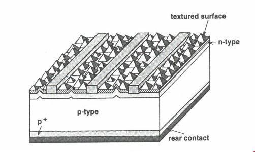
Figure 7: Schematic illustration of the structure of a conventional single crystal silicon solar cell.
(67) The conventional, commercially available silicon solar cell, as at November 2007, of the structure described above is referred to below as a Conventional Solar Cell. This solar cell design is also generally referred to by Skilled Persons in the Field as a back surface field, or BSF, solar cell.
(68) Another family of solar cell structures that was well known to Skilled Persons in the Field, was the Passivated Emitter and Rear Cell (PERC). PERC cells were being researched in laboratories but were not commercialised at that time. PERC cells were developed by the University of New South Wales well prior to November 2007. In these solar cells, the front side is the same as described above for Conventional Solar Cells. However, the rear side of a PERC cell as at November 2007 was, and still is today, mostly covered with a passivating dielectric, with local openings in the dielectric layer for the metal contacts. The entire rear surface was then usually covered with a metal. The PERC structure provides improved rear surface passivation, allowing higher voltages and currents to be achieved. It also improves the reflective properties of the rear, allowing a further boost in the current. Figure 8 below provides a schematic illustration of the general structure of the rear of a PERC cell, shown with silicon oxide as the rear dielectric layer and the metal contacts as “point” contacts.
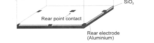
Figure 8: Schematic diagram of the rear of a PERC cell (the front, sun-facing surface of the cell is not shown).
(69) As at November 2007, Skilled Persons in the Field were aware that a particular type of PERC cell was a PERL (Passivated Emitter and Rear Locally doped) silicon solar cell. PERL cells were also developed by the University of New South Wales prior to November 2007 and held the efficiency record for crystalline silicon for some time. In a PERL cell, most of the front and rear surfaces of the silicon are passivated by a dielectric film, except for the regions where electrical contact is made. The silicon regions underneath the rear contacts are heavily doped while the silicon regions underneath the dielectric are not. The general structure of a PERL cell as at November 2007, shown with an oxide film as the front and rear dielectric, is schematically illustrated in Figure 9 below. It is worth noting that other acronyms were also in use at the time to refer to the same type of solar cell structure; for example, the Fraunhofer Institute used the terms Local Back Surface Field (LBSF), since they used aluminium doping to form the local p+ regions.
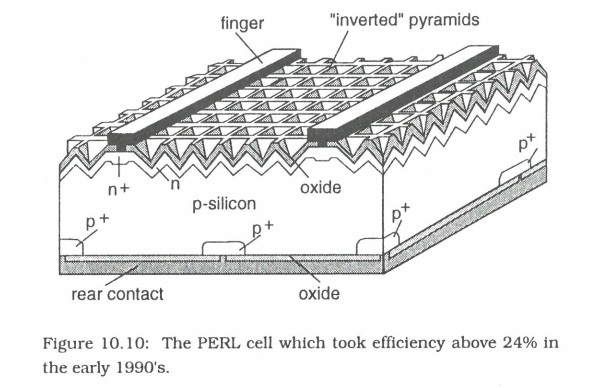
Figure 9: Schematic diagram of the general structure of a PERL cell.
(70) A number of other solar cell structures were well known by other Skilled Persons in the Field:
(a) Interdigitated Back Contact solar cells (IBCs). These solar cells do not have any contacts on the front (sun-facing surface) of the solar cell. In an IBC cell, the emitter covers part (but not all) of the rear surface. The contacts to the p and n regions of the cell alternate along the rear surface to form an interdigitated finger pattern. The general structure of an IBC cell as at November 2007 is schematically illustrated in Figure 10 below.
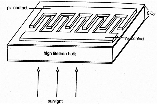
Figure 10: Schematic diagram of the structure of an interdigitated back contact solar cell.
(b) Heterojunction solar cells. These were developed in Japan and relied on the use of doped amorphous silicon to create a pn junction. Heterojunction cells generally do not employ diffusions. Heterojunction cells are based upon amorphous silicon, which was at November 2007, and also is today, the dominant heterojunction cell technology. They employ undoped, heavily doped n-type and heavily doped p-type amorphous silicon layers to create the contact regions for the n and p contacts. The general structure of a heterojunction cell as at November 2007 is schematically illustrated in Figure 11 below.
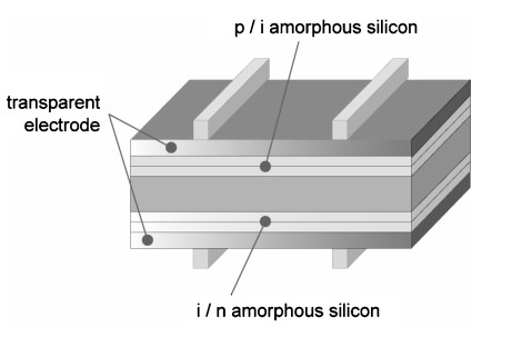
Figure 11: Schematic illustration of the general structure of a heterojunction cell.
(71) Prior to November 2007, silicon solar cells were also being developed and researched that featured more than one dielectric film on the front surface of the silicon. Such dielectric stacks could be used to further improve the optical and/or electronic properties of the solar cell. The use of stacks in semiconductor research, including silicon solar cell research, was generally well known to Skilled Persons in the Field as at November 2007. Prior to 2007, an example of the use of a stack in photovoltaics research was the use of stacks consisting of a thin layer of intrinsic (undoped) amorphous silicon combined with a thicker layer of doped amorphous silicon on top of a silicon wafer to create a high efficiency heterojunction solar cell. In this case, the intrinsic amorphous silicon layer serves primarily to ensure good surface passivation, while the doped amorphous silicon layer ensures good carrier transport. Yet another layer, of a conductive transparent material such as indium tin oxide, is needed on top of the doped amorphous silicon layers to provide lateral conductivity and antireflection.
(72) The final structure of a particular stack was as at November 2007, often a product of experimentation, modelling and analysis, with different techniques and materials, depending upon a number of considerations, which must be weighed against each other.
(73) Solar modules, also known as solar panels, include many individual solar cells that are electrically interconnected. As at November 2007, a solar module typically consisted of a glass coversheet, an encapsulant material (e.g. ethyl vinyl acetate (EVA)), the electrically connected solar cells, a rear sheet of suitable material such as tedlar (a plastic material chosen for its properties in terms of providing a degree of electrical insulation and environmental protection), a frame and a junction box. The structure of a typical solar module as at November 2007 (without the frame and junction box) is schematically illustrated in Figure 12 below.
Figure 12: A typical solar module structure shown without the frame or junction box.
4. Solar cell manufacturing process
(74) As at November 2007, most Conventional Solar Cells were made from either a multi-crystalline or single crystal p-type silicon wafer. The first step was the formation of the silicon wafer. This was achieved by producing a silicon ingot formed from molten silicon, which was then sliced into thin wafers. In the case of a single crystal p-type Czochralski silicon wafer, the first step in manufacturing a silicon solar cell was to remove any damage caused to the silicon wafer from the sawing process used during its preparation from an ingot. Such damage consisted of defects in the near-surface region of the wafer, which could result in increased recombination and would therefore be detrimental to the performance of the cell (that is, its efficiency) if they were not removed. The removal of this damage involved etching the surface of the silicon wafer with an aqueous alkaline solution containing sodium hydroxide or potassium hydroxide and various additives. The etching process removed some of the silicon over the entire wafer surface on both sides of the wafer. In addition, it resulted in the formation of randomly positioned pyramids of varying sizes on the front and rear of the silicon substrate. In the case of a multicrystalline wafer, which was more common, the first steps were similar but not identical, as this was done with using a mixture of hydrofluoric acid (HF) and nitric acid (HNO3) and did not produce pyramidal textures. The front (sun-facing) side of the wafer was then subjected to texturing. This process was used to roughen the surface of the wafer, which improves its optical properties (ie, the amount of light it absorbs).
(75) Following the alkaline etch, the wafer was cleaned to ensure a bare silicon wafer surface that was, as far as possible, free of metallic contaminants and any oxide that had developed during the cleaning steps themselves or on exposure of the silicon wafer to air. Any such oxide that formed was typically a few nanometres thick. The cleaning process used could vary but, when done in industry, typically involved rinsing the silicon wafer in deionised water (high purity water, from which metallic ions and other organic and inorganic contaminants have been removed) to remove as much of the etching solution as possible; immersing the wafer in hydrochloric acid solution or sulphuric acid solution, which may have contained other additives; conducting a further rinse of the wafer in deionised water; immersing the wafer in hydrofluoric acid; conducting a further rinse in deionised water; and finally drying the wafer in hot air.
(76) The next step was a phosphorus diffusion to create regions of n-type silicon to form an n-type phosphorus emitter and pn junction. This process typically involved placing the silicon wafers vertically in a quartz boat which was then placed in a furnace tube heated to a temperature of between about 800-900 °C. A nitrogen carrier gas was bubbled through phosphorus oxychloride (POCl3), resulting in gaseous phosphorus oxychloride, which was then mixed with oxygen and injected into the furnace tube. This resulted in the deposition of phosphorus pentoxide (P2O5) onto the wafer surface. During a subsequent step, the temperature in the furnace was increased to about 900-950 °C. This drove the phosphorus in the P2O5 into the silicon wafer. Alternatively, industrial manufacturers used a conveyor belt furnace to achieve the phosphorus diffusion from a phosphorus containing layer previously deposited on the wafers.
(77) The diffusion process resulted in a phosphosilicate glass on the front surfaces of the wafer. This was typically removed by etching the wafer in hydrofluoric acid. The wafers were subsequently removed from the furnace and a “phosphorus glass” layer that is formed during the diffusion process was removed. This typically involved immersing the wafer in a solution containing hydrofluoric acid.
(78) Removal of the phosphorus glass could be evidenced by the lack of any film of solution forming on the wafer surface when it was pulled out of the solution. This effect is due to the bare surface of the silicon wafer being hydrophobic.
(79) The diffusion process also occurred on all sides of the wafer. As such, in some cases the rear side of the wafer was then etched away using a mixture of HF and nitric acid (HNO3) to remove the n-type region. Typically this would be done with the same tool as was used to remove the phosphosilicate glass. However, single-sided etching processes were relatively difficult to control, and because in the process of the formation of the back surface field the silicon surface containing the phosphorous diffusion was dissolved in the aluminium, it was not critical to remove the n-type doping completely from the rear side. As such, in some cases this step was not done. It was, however, more important to remove any “wraparound” n-type doping on the other sides of the wafer (ie, any n-type region running from the front to the back of the wafer). At the Relevant Date, this was commonly done by laser cutting a trench around the edge of the wafer.
(80) The antireflection coating, a layer of silicon nitride, was deposited on the front side of the wafer. This was generally done by way of PECVD. The next step was the deposition of a film of silicon nitride on the side of the wafer with the diffusion (the front side), which was usually conducted using a PECVD process, as discussed in paragraph 60-61 above. At November 2007, the typical thickness of the PECVD silicon nitride film deposited on the front side of a silicon solar cell was approximately 70-80 nm.
(81) Following the deposition of the silicon nitride film, the next step was to screen print a silver paste on the front side of the wafer to form the metal fingers (front metal contacts). That was followed by a drying step to remove most of the organic solvents from the paste. An aluminium silver paste was then screen printed onto the rear of the wafer to form the rear busbars (regions that could be soldered to for the purpose of attaching ribbons when producing solar cell modules). A further drying step then occurred. An aluminium paste was then screen printed over the rear surface of the wafer, to form the rear side metal contact, followed by another drying step.
(82) The next step in the process was a firing of the wafer. In this step, the wafers moved through a furnace that consisted of several heating zones, the temperature of which could be independently controlled. By adjusting the heat intensity and the speed at which the wafers moved through the furnace, the temporal temperature profile that the wafers experienced could be controlled. Temperatures of a maximum of approximately 800-900 °C were typically used in the firing step, although the peak temperature was only maintained for a short period of time (several seconds). The entire firing step generally lasted around a minute in length.
(83) This process was used to form the contact between the front and rear contacts and the silicon wafer, although in the case of the rear contact, this also drives the aluminium into the rear surface of the wafer. The firing step also has other effects on the structure of the solar cell. At the front surface, the firing step burned the metal contacts (fingers) through the silicon nitride film so that the metal contacted the silicon wafer and reacted with the silicon wafer surface. The metal pastes used to form the contacts have ingredients that enable the paste to etch through the antireflection coating during the firing step. This resulted in electrical contact between the silicon wafer surface and the metal layer. At the rear surface, the firing process resulted in an alloying of the aluminium with the silicon to produce a silicon layer that was heavily doped with aluminium. This produced an electrical contact between the silicon substrate and the rear metal and provided a degree of surface passivation to the rear surface.
(84) The firing process would also release hydrogen from the silicon nitride film, some of which diffused into the bulk of the wafer where it could help to passivate defects and some of which diffused to the silicon/silicon nitride interface to passivate interface defects. In the case of multicrystalline silicon wafers, such bulk hydrogenation was regarded as an important advantage of using PECVD to deposit the silicon nitride layer.
(85) The cells were then tested by measuring the current/voltage curve to obtain the efficiency and were sorted according to their performance (efficiency).
NSD 458 of 2019 | |
SOL DISTRIBUTION PTY LTD ABN 53 146 905 286 | |
Third Cross-Claimant: | BAYWA R.E. SOLAR SYSTEMS PTY LTD ACN 614 035 620 |
HANWHA SOLUTIONS CORPORATION (REGISTRATION NO. 110111-0360935) |