
FEDERAL COURT OF AUSTRALIA
Nichia Corporation v Arrow Electronics Australia Pty Ltd [2015] FCA 699
IN THE FEDERAL COURT OF AUSTRALIA | |
Applicant | |
AND: | ARROW ELECTRONICS AUSTRALIA PTY LTD ACN 065 151 626 Respondent |
AND BETWEEN: | ARROW ELECTRONICS AUSTRALIA PTY LTD ACN 065 151 626 Cross-Claimant |
AND: | NICHIA CORPORATION Cross-Respondent |
JUDGE: | YATES J |
DATE OF ORDER: | |
WHERE MADE: |
THE COURT ORDERS THAT:
1. The parties are to bring in draft orders giving effect to these reasons by 4.00 pm on 17 July 2015.
2. If the parties cannot agree on the question of costs, the respondent is to provide a draft of the order it seeks in that regard, supported by written submissions not exceeding three pages.
3. Any question of costs is to be determined on the papers.
Note: Entry of orders is dealt with in Rule 39.32 of the Federal Court Rules 2011.
NEW SOUTH WALES DISTRICT REGISTRY | |
GENERAL DIVISION | NSD 558 of 2014 |
BETWEEN: | NICHIA CORPORATION Applicant |
AND: | ARROW ELECTRONICS AUSTRALIA PTY LTD ACN 065 151 626 Respondent |
AND BETWEEN: | ARROW ELECTRONICS AUSTRALIA PTY LTD ACN 065 151 626 Cross-Claimant |
AND: | NICHIA CORPORATION Cross-Respondent |
JUDGE: | YATES J |
DATE: | 10 JULY 2015 |
PLACE: | SYDNEY |
REASONS FOR JUDGMENT
Introduction
1 The applicant, Nichia Corporation, is the patentee of Patent No. 720234 (the patent). The relevant specification (AU 199736355 C) is entitled “Light emitting device and display device” (the 355 specification or, where convenient, the specification).
2 The applicant sues the respondent, Arrow Electronics Australia Pty Ltd, for infringement of claim 3 of the specification. Claim 3 is dependent on claim 1.
3 Claim 1 is:
A light emitting device, including a light emitting component and a phosphor capable of absorbing a part of light emitted by the light emitting component and emitting light of wavelength different from that of the absorbed light; wherein said light emitting component comprises a nitride compound semiconductor and said phosphor contains a garnet fluorescent material including at least one element selected from the group consisting of Y, Lu, Sc, La, Gd and Sm, and at least one element selected from the group consisting of Al, Ga and In, and being activated with cerium.
4 Claim 3 is:
A light emitting device according to claim 1, wherein the phosphor contains fluorescent material represented by a general formula (Re1-rSmr)3(All-sGas)5O12:Ce, where 0<r<1 and 0<s<1 and Re is at least one selected from Y and Gd.
5 The respondent has cross-claimed seeking revocation of claims 1 and 3, on various grounds. A threshold question has arisen as to the correct priority date of each claim.
6 The applicant says that claims 1 and 3 each define more than one form of the invention. It says that each form of the invention in claim 3 is entitled to a priority date of 29 July 1996 based on the disclosures in Japanese patent application JP8-198585 (JP585), one of the priority documents identified in the 355 specification. As to claim 1, the applicant says that many of the forms of the invention defined therein are entitled to a priority date of 29 July 1996 based on the disclosures in JP585, some forms are entitled to a priority date of 17 September 1996 based on the disclosures in Japanese patent application JP8-244339 (JP339) (another priority document identified in the 355 specification), and the remainder of the forms of the invention are entitled to a priority date of 29 July 1997, being the filing date of the application for the patent.
7 The respondent says that the priority date of claim 1 is 29 July 1997 because the invention, as so claimed, is not divisible into different forms and was first disclosed in the application for the patent. The respondent says that the invention in claim 3 is limited to a subset of fluorescent materials disclosed in claim 1 and, as it is dependent on claim 1, claim 3 is only entitled to the same priority date as claim 1.
8 As the determination of the priority date of claims 1 and 3 will have an important impact on how the respondent’s challenge to the validity of the claims should proceed, I have ordered that the question of the correct priority date of claims 1 and 3 be determined separately from and prior to any other question in the proceeding (the separate question): r 30.01 of the Federal Court Rules 2011.
Scientific background
9 The parties have prepared a primer for use in determining the separate question. It reflects the parties’ agreed understanding of the meaning of a number of terms and concepts. I have admitted the primer into evidence as Exhibit C, subject to a limitation under s 136 of the Evidence Act 1995 (Cth) that its use is to be confined to construing the specification and claims, and the priority documents relied upon by the applicant.
10 The following summary of the scientific background is based substantially on the agreed primer.
Chemical notation
11 In chemical notation:
(a) Y represents the element yttrium;
(b) Lu represents the element lutetium;
(c) Sc represents the element scandium;
(d) La represents the element lanthanum;
(e) Gd represents the element gadolinium;
(f) Sm represents the element samarium;
(g) Al represents the element aluminium;
(h) Ga represents the element gallium;
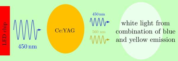
(i) In represents the element indium;
(j) O represents the element oxygen;
(k) Ce represents the element cerium; and
(l) Si represents the element silicon.
Light emission
12 Electromagnetic radiation is the name for energy that is propagated by waves of electromagnetic fields. Photons are the elementary particles of electromagnetic radiation.
13 Electromagnetic radiation covers photon energies that are very high and have very short wavelengths (for example, x-rays), down to energies that are low and have very long wavelengths (for example, microwaves and radio waves).
14 The term “light” is often used to refer to electromagnetic radiation that is visible to humans. The term also includes radiation that is adjacent to visible light in the electromagnetic spectrum, such as ultraviolet light and infrared light.
15 Electrons present in atoms may exist in different energy states. The lowest energy state is termed the “ground state”. Other energy states are referred to as “excited states”. The relaxation transitions of excited electrons in atoms are a common source of luminescence.
16 Luminescence is the emission of electromagnetic radiation where the excitation process is not due to heat.
17 Photoluminescence is the emission of light after the absorption of photons. When a photon is absorbed, the electron is excited to a higher energy state. Light emission is one of the ways in which the electrons can return to their ground state.
18 The wavelength of the absorbed light is determined by the energy difference between the two states of the transition. Similarly, the wavelength of the emitted light is determined by the energy difference between the two states of the transition. Usually, but not in every case, the light emitted is of a different wavelength to the light absorbed.
19 Fluorescence is photoluminescence in which a photon is absorbed by a substance (for example, an atom, ion or molecule) and a photon is emitted from that substance. The wavelength of the omitted photon is usually longer than the wavelength of the absorbed photon.
Diodes
20 A diode is an electronic component with two terminals. Most electronic diodes are made with semiconductor materials.
21 Diodes have low resistance to electrical current in one direction (the forward direction) and high resistance in the other direction (the reverse direction). In effect, this means that diodes conduct electrical current only in the forward direction.
22 A light emitting diode is a particular design of a diode where the forward current is turned into light emission. In other words, the diode produces luminescence. Not all semiconductor diodes are light emitting diodes.
Semiconductors
23 A semiconductor is an element or compound used in electrical powered devices that has a degree of electrical conductivity somewhere between an electrical insulator and an electrical conductor. Some semiconductor devices (such as a light emitting diode) can produce luminescence.
24 Compound semiconductors comprise two or more elements. The precise ratios of the elements must remain uniform throughout the compound semiconductor. A particular compound can be a semiconductor even though its constituent elements are not semiconductors.
25 A nitride compound semiconductor is linked to the family known as the group-III nitrides. Al, Ga and In are metal elements from group-III of the periodic table. They have similar but not identical chemical properties. The nitride compound semiconductors form when Al, Ga, or In chemically bond to N in a 1:1 ratio to form a crystal structure that has semiconducting properties. In addition to the three binary compounds (AlN, GaN, InN), mixtures can be made. For example, InxGa1-xN is a nitride compound semiconductor, being a mixture of InN and GaN, where the ratio of InN and GaN is determined by x.
Phosphors
26 A phosphor is a substance that exhibits luminescence when suitably excited.
27 Phosphors often have two components. The first is the luminescent centre, sometimes called the dopant or activator (I will use the term “activator”). The second is the host matrix or host crystal lattice (I will use the term “host matrix”). The activator is usually a particular element, which will often be in an ion form in the host matrix.
28 In general, the host matrix does not absorb visible light and therefore cannot act as a phosphor, until it is “activated” by a suitable substance. The activator is deliberately chosen to have absorption and emission energies required for a particular application. In general, the activator does not influence the host matrix, as it is included in low concentrations and is chemically compatible with atoms of the host matrix. However, the energies (or wavelengths) of the electronic transitions of activator atoms are influenced by the host matrix. Thus, for a given activator, the exact wavelengths of absorption and emission will change with different host matrixes.
29 Ce is an activator.
30 The general role of a phosphor, when used with a light emitting diode, is to change the overall emission wavelengths emitted from the integrated device. It achieves this by the activator absorbing photons emitted by the light emitting diode semiconductor to produce excited states of the activator. The activator subsequently relaxes back to its original ground state by emitting photons of a different energy, and hence of a different colour to that absorbed. A key requirement of the phosphor is having an activator with absorption transitions that match the light emitting diode emission, and having emission transitions at energies corresponding to the desired new colours.
Garnet
31 Garnet is a general classification name for a class of natural gemstones that have oxygen forming tetrahedra with Si at the centre. The general chemical formula for a natural garnet is X3Z2(SiO4)3.
32 In addition to natural garnets, a number of synthetic garnets have been fabricated following the same general chemical formula given above. One such synthetic garnet is YAG – an acronym for yttrium aluminium garnet. YAG is represented by the chemical formula Y3Al5O12 which can be written in the general garnet formula as Y3Al2(AlO4)3.
33 Garnets are crystalline materials. This means the elements in the garnet structure have a periodic arrangement. At the heart of a crystal structure is a single unit that represents the repeating pattern of the crystal.
The 355 specification
34 The 355 specification describes the invention as one relating to a light emitting diode used in a light emitting device, comprising a phosphor which converts the wavelength of light emitted by a light emitting component, and emits light.
35 The specification describes the benefits of light emitting diodes as follows:
A light emitting diode is compact and emits light of clear color with high efficiency. It is also free from such a trouble as burn-out and has good initial drive characteristic, high vibration resistance and durability to endure repetitive ON/OFF operations, because it is a semiconductor element. Thus it has been used widely in such applications as various indicators and various light sources. Recently light emitting diodes for RGB (red, green and blue) colors having ultra-high luminance and high efficiency have been developed, and large screen LED displays using these light emitting diodes have been put into use. The LED display can be operated with less power and has such good characteristics as light weight and long life, and is therefore expected to be more widely used in the future.
36 The specification discloses that various attempts have been made to make white light sources using light emitting diodes. It explains that, although light emitting diodes are effective as light emitting devices for generating individual colours, such as red, green and blue, a satisfactory light source capable of emitting white light by using light emitting components has not been obtained.
37 The specification discloses that the applicant has developed light emitting diodes which convert the colour of light, emitted by light emitting components, using certain fluorescent materials disclosed in certain Japanese patents. The specification teaches, however, that these arrangements have certain problems, including the deterioration or degradation of the fluorescent material.
38 The present invention is said to provide an alternative to known light emitting devices and displays. It aims to alleviate at least one of the problems referred to in the specification and provides a light emitting device which experiences only extremely low degrees of deterioration in emission light intensity, light emission efficiency and colour shift over a long time of use, with high luminance.
39 The specification contains the following teaching:
Generally, a fluorescent material which absorbs light of a short wavelength and emits light of a long wavelength has higher efficiency than a fluorescent material which absorbs light of a long wavelength and emits light of a short wavelength. It is preferable to use a light emitting component which emits visible light than a light emitting component which emits ultraviolet light that degrades resin (molding material, coating material, etc.). Thus for the light emitting diode of the present invention, for the purpose of improving the light emitting efficiency and ensure long life, it is preferable that main emission peak of the light emitting component be set within a relatively short wavelength range of 400 nm to 530 nm in the visible light region, and main emission wavelength of the phosphor be set to be longer than the main emission peak of the light emitting component. With this arrangement, because light converted by the fluorescent material has longer wavelength than that of light emitted by the light emitting component, it will not be absorbed by the light emitting component even when the light emitting component is irradiated with light which has been reflected and converted by the fluorescent material (since the energy of the converted light is less than the band gap energy). Thus the light which has been reflected by the fluorescent material or the like is reflected by the cup wherein the light emitting component is mounted, making higher efficiency of emission possible.
(Errors in original.)
40 The specification describes a first embodiment of the invention, which is a light emitting diode that employs a gallium nitride compound semiconductor element, which is capable of emitting blue light, in combination with a garnet phosphor activated with Ce. When activated, the phosphor is excited by the blue light emitted by the semiconductor element and emits yellow light. The blue light and the yellow light blend to produce white light: see [49]-[50] below.
41 For this embodiment, the specification expresses a preference for a phosphor which is an yttrium-aluminium-garnet fluorescent material (a YAG phosphor) activated with Ce. The fluorescent material having the general formula set out in claim 3 is specifically referred to.
42 The specification teaches that the wavelength of the emitted light can be shifted to a shorter wavelength by substituting part of the Al in the phosphor with Ga. The specification also teaches that the wavelength of the emitted light can be shifted to a longer wavelength by substituting part of Y in the semiconductor with Gd. In this way, the colour of the emitted light can be changed.
43 Claims 1 and 3 are set out at [3]-[4].
44 Claim 3 defines fluorescent material that is represented by the general formula (Re1-rSmr)3(All-sGas)5O12:Ce, where 0<r<1 and 0<s<1 and Re is at least one selected from Y and Gd. This general formula represents a general description of the composition of a synthetic garnet structure. The formula unit identifies the ratio of oxygen ions (12) to “large” metal ions (3), identified by the notation (Rel-rSmr), to “small” metal ions (5), identified by the notation (Al1-sGas). The notation “:Ce” refers to Ce as an activator. Therefore, the general formula represents a Ce-activated phosphor with a garnet structure.
45 The general formula includes (All-sGas)5 where 0<s<1. The parameter s describes the fraction of Ga present. For example, s = 0.2 would mean 20 out of every 100 of (Al + Ga) would be Ga. The parameter s can be 0 or 1. This means that the formula covers the possibility of having only Al (and no Ga), or only Ga (and no Al) present in material represented by the formula.
46 The general formula includes (Rel-rSmr)3 where 0≤r<1 and Re is at least one selected from Y or Gd. The parameter r represents the fraction of Sm present. The general formula provides that:
(a) the material cannot contain only Sm (ie, crystals represented by the formula Sm3(All-sGas)5O12, are not included in the general formula); and
(b) there must always be some atoms of either Y or Gd (or both) present.
47 The inclusion in the general formula of the words “at least one” implies that both Y and Gd can be present. This means that the possible combinations of elements represented by this portion of the general formula are:
(a) Y;
(b) Gd;
(c) Y and Gd;
(d) Y and Sm;
(e) Gd and Sm; and
(f) Y, Gd and Sm.
48 An example of a material represented by the general formula in claim 3 is Y3Al5O12:Ce. This material may be identified as YAG:Ce where Ce is the activator of the phosphor.
49 The parties agree that YAG:Ce can absorb specific wavelengths of light that correspond to exciting Ce electrons to higher energy states. One wavelength for absorption in YAG:Ce is blue light of 450 nanometres. A nanometre (nm) is a unit of spatial measurement that is 10-9 metre, or one billionth of a metre. After being excited by this absorption process, the Ce electrons return to lower energy states by the complementary process of photoluminescence. This emitted light has a different wavelength to the absorbed light. When YAG:Ce is excited by a blue light, the phosphor emits an emission peak that spans the wavelength range from around 500 to 700 nm. The human eye perceives this phosphor emission as yellow light, which can, when combined with blue light emitted by the LED, make the total light emitted appear to the eye as white light. This is because the total has the three red, green and blue components of the primary colours.
50 The diagram below (not in the 355 specification) illustrates how this works. Blue light at 450 nm enters the YAG:Ce phosphor, is absorbed, and yellow light is emitted. As the absorption by the phosphor is less than 100%, some 450 nm blue light is also transmitted through and around the phosphor. The totality of light exiting the device is 450 nm from transmission from the light emitting diode (that is not absorbed by the phosphor) and light in the wavelength range from around 500 to 700 nm from emission of the phosphor.
Legal framework
The legislation
51 The Patents Act 1990 (Cth) (the Act) provides that each claim of a specification must have a priority date: s 43(1). The priority date is the date of filing of the specification or, if the Patents Regulations 1991 (Cth) provide for the determination of a different date, the date determined under the regulations: s 43(2).
52 Where a claim defines more than one form of an invention, then, for the purposes of priority date determination, the claim must be treated as if there were a separate claim for each form of the invention that is defined: s 43(3). The priority date of a claim of a specification may be different from the priority date of any other claim of the specification: s 43(4).
53 The parties agree that the form of reg 3.12 applicable to the separate question is:
3.12 Priority dates generally
(1) Subject to regulations 3.13 and 3.14 and subregulation (2), the priority date of a claim of a specification is the earliest of the following dates:
(a) the date of filing of the specification;
(b) if the claim is fairly based on matter disclosed in 1 or more priority documents, the date of filing the priority document in which the matter was first disclosed;
…
(2) For the purposes of paragraph 1(b):
…
(a) If:
(i) the application that relates to the specification containing the claim is a PCT application that, under Article 8 of the PCT, claims the priority of an earlier application; and
(ii) that earlier application is:
…
(B) a basic application, made not more than 12 months before the international filing date of the PCT application, that is the first application made in a Convention country in respect of the invention;
…
that earlier application, and a specification filed in relation to that earlier application after it was made, are priority documents.
…
(2B) A reference in subregulation (2) to a basic application does not include a basic application that has been disregarded by the Commissioner under section 96 of the Act.
…
54 The respondent accepts that JP585 and JP339 are basic applications for the purposes of reg 3.12(2)(c)(ii)(B). The respondent also accepts that reg 3.12(2) requires an identification of the priority document which first discloses matter which affords the fair basis for the claim.
The legal test
55 Regulation 3.12(1)(b) speaks of a claim that is fairly based “on matter disclosed in 1 or more priority documents”. The parties accept that the standard to be applied when considering whether a claim is fairly based is that referred to in Lockwood Security Products Pty Limited v Doric Products Pty Limited (2004) 217 CLR 274 at [69], namely that there be “a real and reasonably clear disclosure” of the claimed invention.
56 In Vehicle Monitoring Systems Pty Ltd v Sarb Management Group Pty Ltd (t/as Database Consultants Australia) (No 2) (2013) 101 IPR 496 at [122], I pointed out that the test of fair basis for determining the priority date of a claim is not the same as the test for fair basis under s 40(3) of the Act, which concerns claim width and is directed, in a general sense, to ensuring internal consistency between that which is described as the invention, and that which is claimed as the invention. This difference is reflected in the language of s 40(3), which requires that a claim be fairly based on “the matter described in the specification”. In reg 3.12(1)(b), the inquiry is whether the claim is fairly based on “matter disclosed”. The significance of the omission of the definite article “the” in relation to “matter” in the test applied under reg 3.12(1)(b) was specifically referred to and discussed in Leonardis v Sartas No 1 Pty Ltd (1996) 67 FCR 126 at 139, where the Full Court made clear that some part or parts of the overall disclosure made in the relevant priority document can provide “matter” on which a claim can be fairly based for the purpose of assigning a priority date to the claim.
57 Regard should also be had to the use of the word “disclosed” in reg 3.12(1)(b), contrasted with the word “described” in s 40(3). The word “described” as used in s 40(3) focuses attention on the invention that is required to be fully described in the specification: see s 40(2). However, in its particular context, the word “disclosed” in reg 3.12(1)(b) is a more general expression which, in conjunction with the word “matter”, reinforces that priority can be claimed by reference to some part or parts of the priority document.
Do claims 1 and 3 define more than one form of the invention?
Relevant case law
58 The plurality in AstraZeneca AB v Apotex Pty Ltd (2014) 226 FCR 324 at [250] briefly discussed the history of s 43(3) of the Act and its predecessor provision in the Patents Act 1952 (Cth), noting that these provisions were included to overcome the ruling in Thornhill’s Application [1962] RPC 199.
59 In Thornhill’s Application, consideration was given to the drafting of the following claim. It should be noted that the indices (a), (b)(i), (b)(ii), (c) and (d) were added to the claim at the hearing before the Hearing Officer in that case to illustrate the argument made. The indices did not appear in the printed specification:
1. A method of producing a black tea concentrate (a) which consists in cutting, grinding, or otherwise finely dividing fresh green leaves of the tea tree, and (b) oxidising the comminuted particles either (i) by exposing the raw mass to the action of the oxygen of the air until the mass becomes dark brown in colour and subsequently extracting by boiling water or steam the water-soluble constituents of the leaves, or (ii) initially after comminuting the leaves extracting in the same way by percolation the soluble constituents of the leaves and introducing into the obtained solution a minute quantity of an oxidising inorganic substance, (c) subjecting the solution obtained in either way to heating in the open air at a temperature approaching the boiling point of water for a duration up to six hours until the required degree of oxidation is attained and until as a result of heating there occurs the polymerisation of the tannin compounds polyphenol and catechol with constituents of the solution and the solution has lost its bitter taste inherent in the solution of the constituents of the green tea leaf, and (d) evaporating excess water.
60 The Hearing Officer described the claim as follows:
It will be noted that claim 1 embodies two alternatives, i.e. it may be regarded as two claims 1A and 1B, wherein:—
1A = a + b(i) + c + d
and the method which may be represented as
1B = a + b(ii) + c + d
61 The Hearing Officer concluded that, as the claim could be regarded as two notional claims, each notional claim could be afforded its own priority date. However, on appeal, Lloyd-Jacob J concluded (at 207) that there was no provision in the Patents Act 1949 (UK) that would warrant the attribution of two different priority dates to different parts of the one claim.
62 In AstraZeneca, one of the claims in question (claim 1 of what was called the 842 or cation patent) was as follows:
1. A pharmaceutical composition comprising [rosuvastatin] or a pharmaceutically acceptable salt thereof as the active ingredient and an inorganic salt in which the cation is multivalent, provided that:
(i) the inorganic salt is not hydrotalcite or synthetic hydrotalcite; and
(ii) the counter anion to the inorganic salt is not a phosphate.
63 At [251], the plurality concluded (Jessup J agreeing at [447]):
251 In our view, claim 1 of the 842 or cation patent does not define more than one form of the invention. Unlike the claim in issue in Thornhill’s Application, claim 1 of the 842 or cation patent does not by its terms allow for any alternatives or, adopting the language of s 43(3), different forms of the same invention. Claim 1 defines only one form of the invention even though there will be any number of potential variants that are within its scope. We do not think s 43(3) is intended to treat every potential variant of the defined invention as if it was a form of the invention that must be treated as a separate claim which is to be given its own priority date. Rather, it is intended to deal with very different situations such as that which arose in Thornhill’s Application or where, to take a slightly different example, a claim is dependent on one or more independent claims (claim 3 of the 842 or cation patent takes this form) each of which has a different priority date. We therefore reject AstraZeneca’s submission based upon s 43(3) of the Act.
(Emphasis in original.)
64 The corresponding provision in the United Kingdom is s 125 of the Patents Act 1977 (UK). Section 125 relevantly provides:
125 Extent of invention
(1) For the purposes of this Act an invention for a patent for which an application has been made or for which a patent has been granted shall, unless the context otherwise requires, be taken to be that specified in a claim of the specification of the application or patent, as the case may be, as interpreted by the description and any drawings contained in that specification, and the extent of the protection conferred by a patent or application for a patent shall be determined accordingly.
(2) It is hereby declared for the avoidance of doubt that where more than one invention is specified in any such claim, each invention may have a different priority date under section 5 above.
…
65 In Miller R, Burkill G, Birss C and Campbell D, Terrell on the Law of Patents (17th ed, Sweet and Maxwell, 2011), the authors state (at 7-12):
When can a claim have multiple priorities?
7-12 If a claim is drafted in such a way that it encompasses clear alternatives—for example, a claim which defines a chemical compound by reference to a structure which may take identified alternative forms—then attributing multiple priorities is unlikely to cause difficulty. In effect, the claim can be regarded as being made up of several discrete claims or—in the words of section 125(2) —as specifying more than one invention, each with a different priority date. However, it is difficult to see how a broad claim which does not set out alternatives as such could be regarded as specifying more than one invention, and it is hard to see how such a claim could allow for multiple priorities to be claimed. This is in line with the approach taken by the European Patent Office.
(Citations omitted.)
66 Section 125(2) of the Patents Act 1977 (UK) was considered in Hallen Company v Brabantia (UK) Ltd [1990] FSR 134. In that case, a particular claim (claim 9) claimed “an apparatus according to any preceding claim”. Aldous J construed the claim as being a number of discrete claims, and not a composite claim. At 140, Aldous J said:
The use of the words “apparatus according to any preceding claim” is a shorthand way of writing out a large number of claims. For instance, if those words are used in claim 3 of a patent having three claims, what is being claimed, and claimed separately, is the combination of claims 1 and 3 and claims 1, 2 and 3. To hold to the contrary … would mean that the patentees in the future would have to write out each combination as a separate claim which would lead to even more claims in patents than there are now.
67 In Merck & Company (Macek’s) Patent [1967] RPC 157, Lloyd-Jacob J considered an allegation of prior claiming in relation to a number of claims in a granted patent, including the following:
1. A composition having enhanced bactericidal activity comprising novobiocin in combination with at least one other antibiotic selected from the following, namely, penicillin, tetracycline, oxytetracycline, chlortetracycline, streptomycin, chloramphenicol, bacitracin, neomycin, spiramycin, streptothricin and grisein.
68 As to the construction of this claim, Lloyd-Jacob J said:
The claim, it will be seen, is of the comprehensive type permitting of alternative additions to novobiocin, which alternative additions consist of one or more of the named antibiotics. It is a convenient summation of what is in effect a number of separate claims to different compositions of which some will relate to compositions having two ingredients and some to three or more ingredients.
The first notional rewriting of this claim to make plain this differentiation would be: (A) “A composition having enhanced bactericidal activity comprising novobiocin in combination with one other antibiotic selected from the following, namely, penicillin, tetracycline, oxytetracycline, chlortetracycline, streptomycin, chloramphenicol, bacitracin, neomycin, spiramycin, streptothricin and grisein.” (B) “a composition . . . comprising novobiocin in combination with two or more antibiotics selected from the following, namely, penicillin, tetracycline, oxytetracycline, chlortetracycline, streptomycin, chloramphenicol, bacitracin, neomycin, spiramycin, streptothricin and grisein.”
Of these two notional divisions of claim 1 only “A” is relevant and this may be notionally further rewritten in the form of eleven independent claims in the form, (C) “A composition . . . comprising novobiocin in combination with penicillin”; (D) “A composition . . . comprising novobiocin in combination with tetracycline”; (E) “A composition . . . comprising novobiocin in combination with oxytetracycline”; (F) “A composition . . . comprising novobiocin in combination with chlortetracycline”; and so on through the list.
69 Although dealing with prior claiming, Merck provides guidance on how claims of the kind there under consideration are to be construed. The applicant placed reliance on Merck because the relevant claim had drafting similarities to claims 1 and 3 of the 355 specification in that each of these claims provides an explicit selection step leading to various combinations and hence various phosphors within the scope of the claim. The applicant submitted that if the claim in Merck was written out as described by Lloyd-Jacob J, it would comprise 2,047 claims.
70 The applicant also referred to “claim splitting” cases where, in order to avoid the problem posed by Thornhill’s Application, amendments were sought to split a composite claim into various forms of the invention so as to render each as a separate claim with its own priority date. Farbenfabriken Bayer AG’s Patent [1966] RPC 278 and Anderson’s Application [1966] FSR 218 are two such examples. It is not necessary for me to refer to these cases in greater detail.
The parties’ submissions
71 As I have noted, the applicant placed reliance on the selection steps in claim 1 of the 355 specification with respect to the phosphor used in the invention. Those steps are:
selecting at least one element from the group consisting of Y, Lu, Sc, La, Gd and Sm; and
selecting at least one element from the group consisting of Al, Ga and In.
72 The applicant submitted that these steps show that claim 1 defines more than one form of the invention, with the result that, for the purpose of determining priority, the claim must be treated as claiming separate forms of the invention within the meaning of s 43(3) of the Act. It submitted that these selection steps are a convenient summation of what is, in effect, a number of separate claims to different combinations. Some combinations will have two elements; other combinations will have three or more elements. Professor Reeves’ evidence was that the garnet fluorescent material in the phosphor of claim 1 may contain 441 different combinations of elements.
73 The applicant submitted that claim 3 of the 355 specification is drafted in a way that “defines clear alternatives that represent a sub-set of the alternatives in claim 1”. The applicant identified 18 different combinations derived from the selection between Y and Gd and the values assigned to r and s in the general formula. For this purpose, the applicant assigned 0 or 1 for the values of each of r and s.
74 The respondent submitted that, in claim 1 of the 355 specification, there is only one form of the invention, even though there will be “any number of potential variants that are within its scope”. It submitted that claim 1 of the 355 specification “falls fairly within the reasoning” applied by the Full Court in AstraZeneca to the claim there under consideration.
75 The respondent noted that it is common ground between the parties that Lu, Sc and In are not mentioned in the priority documents. The respondent argued that, as none of the priority documents discloses an invention that includes Lu, Sc and In within the groups of elements from which a selection is to be made, and as claim 1 defines only one form of the invention, the priority date of the claim must be the filing date of the patent application, namely 29 July 1997.
76 The respondent treated claim 3 of the 355 specification in the same way. According to the respondent, claim 3 defines only one form of the invention. Further, the respondent submitted that claim 3 has “no alternative roots of dependency” that would attract s 43(3) of the Act.
77 Here, the respondent alluded to the example given in AstraZeneca where s 43(3) might be deployed to assign different priority dates to a claim that is dependent on one or more independent claims. However, the respondent’s submission must be understood as arguing that the example given in AstraZeneca does not apply to the present case. The respondent’s position appears to be that as, on its argument, claim 1 has a priority date of 29 July 1997, claim 3 must have the same priority date because of its dependency on claim 1.
78 This argument appears to be based on how, according to the respondent, claim 3 should be notionally rewritten to reflect its dependency on claim 1. In this connection, the respondent submitted that claim 3 should read:
A light emitting device according to claim 1,
including a light emitting component and a phosphor capable of absorbing a part of light emitted by the light emitting component and emitting light of wavelength different from that of the absorbed light; wherein said light emitting component comprises a nitride compound semiconductor and said phosphor contains a garnet fluorescent material including at least one element selected from the group consisting of Y, Lu, Sc, La, Gd and Sm, and at least one element selected from the group consisting of Al, Ga and In, and being activated with cerium,
wherein the phosphor contains fluorescent material represented by a general formula (Rel-rSmr)3(All-sGas)5O12:Ce, where 0<r<1 and 0<s<1 and Re is at least one selected from Y and Gd.
79 The respondent submitted that, so written, the claim reveals what it called “the root of dependency”. This seems to be because, in this version of claim 3, all the features of claim 1 are imported, even though claim 3 is admittedly narrower in scope than claim 1 because of the selection criteria it provides.
80 By way of contrast, the respondent provided a rewritten version of claim 3 as reflected in the applicant’s submissions:
A light emitting device according to claim 1,
including a light emitting component and a phosphor capable of absorbing a part of light emitted by the light emitting component and emitting light of wavelength different from that of the absorbed light; wherein said light emitting component comprises a nitride compound semiconductor and said phosphor contains a garnet fluorescent material including at least one element selected from the group consisting of Y, Lu, Sc, La, Gd and Sm, and at least one element selected from the group consisting of Al, Ga and In, and being activated with cerium,
wherein the phosphor contains fluorescent material represented by a general formula (Rel-rSmr)3(All-sGas)5O12:Ce, where 0<r<1 and 0<s<1 and Re is at least one selected from Y and Gd.
81 The respondent criticised this version because, according to it, the claim omits various features of claim 1.
82 I do not accept that claim 3 of the 355 specification should be understood as set out in [78]. So written, the claim would contain redundant and confusing wording. The general formula in claim 3 makes clear that the “large” metal ions must include at least one from Y and Gd, and must include Sm, unless the value of r = 0. The “large” metal ions do not include Lu, Sc or La. Similarly, the general formula makes clear that the “small” metal ions involve selections relating to Al and Ga that do not involve In. Writing in references to Lu, Sc, La and In in claim 3, only to have those elements automatically rejected as selection possibilities by the general formula, is a pointless exercise. In any event, I cannot see how claim 3 can be assigned a priority date based on selected combinations arising under claim 1 that are not within the scope of claim 3 itself.
83 Therefore, I reject the respondent’s case to the extent that it rests on its version of claim 3 rewritten to take account of the claim’s dependency on claim 1.
Consideration
84 In AstraZeneca, the Full Court emphasised the terms in which the claim is drafted and directed attention to whether the claim, according to its terms, allows for alternatives.
85 Claim 1 and claim 3 of the 355 specification are cast in terms that are different to the claim considered in AstraZeneca. Claim 1 includes two discrete and express selection steps—one referable to the selection of the “large” metal ions and the other referable to the selection of the “small” metal ions in the fluorescent material—providing for differently constituted phosphors, depending on the selections made and the combinations arrived at.
86 Claim 3, although differently drafted, also contains discrete and express selection steps. Similarly to claim 1, there is a stated, but different, selection with respect to the “large” metal ions in the fluorescent material. The constituents of this material are also determined by the selection of a value for r from the given range. The general formula in claim 3 also provides for a selection in relation to the “small” metal ions of the fluorescent material by providing a range of values for s. These various selection steps combine to provide differently constituted phosphors.
87 I am satisfied that, by their terms, each of claims 1 and 3 of the 355 specification envisage and provide for different forms of the invention, as understood by s 43(3) of the Act. In each case, these forms are represented by the individual phosphors obtained after the selection steps have been undertaken.
The priority dates of the claims
Introduction
88 The respondent accepts that if, as I have found, claim 1 of the 355 specification defines more than one form of the invention, then the priority dates of those forms are the dates that the applicant has identified.
89 As I have found that claim 3 of the 355 specification also defines more than one form of the invention, the question then becomes whether the forms of the phosphor represented by the general formula in that claim are disclosed in JP585. This question focuses attention on the notation (Al,Ga)5 used in claim 1 and claim 2 of JP585, and elsewhere in JP585, where it is stated that the phosphor of the invention therein described is represented by RE3(Al,Ga)5O12:Ce, where RE is at least one selected form Y, Gd and Sm.
90 As originally advanced, the issue that divided the parties was this: Does the notation (Al,Ga)5 as used in the general formula in claim 1 of JP585, denote any mixing of Al and Ga so as to include 100% Al and 0% Ga, and 0% Al and 100% Ga, provided the total number of atoms is conserved to make five atoms (ie, so as to include RE3Al5O12:Ce and RE3Ga5O12:Ce, respectively), as the applicant contends, or does it denote, as the respondent contends, that Al and Ga must each be present in the phosphor, provided, once again, that the total number of atoms is conserved to five atoms?
JP585
91 Claim 1 of JP585 is:
A light emitting diode comprising a LED chip using a gallium nitride compound semiconductor as a light emitting layer and a phosphor which absorbs at least a part of light emitted by the LED chip to emit light by converting the wavelength, wherein a peak of the emission spectrum of the LED chip has an emission wavelength within the range from 400nm to 530nm and the phosphor is represented by RE3(Al,Ga)5O12:Ce, where RE is at least one selected from Y, Gd and Sm.
92 Like the general formula of claim 3 of the 355 specification, the formula RE3(Al,Ga)5O12:Ce in claim 1 of JP585 represents a general description of the composition of a synthetic garnet structure. The formula unit identifies a ratio of oxygen ions to “large” metal ions identified by the notation RE (being at least one selected from Y, Gd and Sm) to “small” metal ions identified by the notation (Al,Ga)5. The ratio of oxygen to “large” metal ions to “small” metal ions is 12 to 3 to 5. The formula represents a Ce-activated phosphor with a garnet structure. The same general formula is used in claim 2 of JP585. Unlike the general formula in claim 3 of the 355 specification, the crystals represented by the general formula in claims 1 and 2 of JP585 may include only Sm (ie, no Y or Gd).
93 Claim 3 is:
A light emitting diode according to claim 1 or 2, wherein the composition of the phosphor is represented by the following general formula:
(Y1-p-q-rGdpCeqSmr)3(Al1-sGas)5O12
where 0<p<0.8
0.003<q<0.2
0.0003<r<0.08
0<s<l
94 It is apparent from the formula in claim 3 of JP585 that the garnet phosphor may contain 0% Al and 100% Ga or 100% Al and 0% Ga because 0<s<l. There is no dispute about that matter.
95 I note in passing that the translation of JP585 in evidence misdescribes the general formula in claim 3 thereof. It is accepted by the parties that the general formula in claim 3 of JP585 is as set out above.
96 I also note in passing that the phosphor defined by the general formula in claim 3 of JP585 is the fluorescent material defined by the general formula in claim 4 of the 355 specification. However, claim 4 of the 355 specification is not in suit.
97 JP585 notes that there are fluorescent materials which convert light of shorter wavelength emitted by a light emitting component into light of longer wavelength, and fluorescent materials which convert light of longer wavelength emitted by a light emitting component into light of shorter wavelength. However, according to JP585, the efficiency of conversion of long-wavelength light into short-wavelength light is extremely low and is not practical. JP585 teaches that the steps taken to improve conversion efficiency can lead to a deterioration of the fluorescent material. JP585 teaches that there are other problems which might lead to a deterioration of the fluorescent material. This deterioration can lead to a colour shift in the emitted light or a blackening of the fluorescent material resulting in a lowered efficiency of extracting light. JP585 says that the invention it describes is intended to solve these various problems and to provide a light emitting diode which is subject only to extremely low degrees of deterioration in light emission efficiency and colour shift over a long period of time, with high luminance.
98 JP585 states:
The present inventors have found, as a result of various experiments, that it is made possible to prevent the decrease in emission efficiency and color shift through operation with a high luminance over a long period of time by selecting a particular semiconductor and a fluorescent material in a light emitting diode which uses a phosphor to convert the color of light emitted by a LED chip having a relatively high radiation energy in visible region, and have achieved the present invention.
The phosphor used in the light emitting diode must satisfy the following requirements:
1. Excellent resistance against light, particularly durability to endure light of a radiation intensity as high as about 30 to 40 times that of sun light, because the fluorescent material is exposed to intense radiation from a tiny region such as a semiconductor light emitting component.
2. Capability to emit light in blue region, not ultra violet, because mixing of colors with the light emitting components is used.
3. Capability to emit light from green to red regions in consideration of mixing with blue light.
4. Good temperature characteristic suitable for location in the vicinity of the light emitting component.
5. Capability to continuously change the color tone in terms of the proportion of composition or ratio of mixing a plurality of fluorescent materials.
6. Weatherability for the operating environment of the light emitting diode.
(Errors in original.)
99 JP585 discloses the following characteristics of the phosphor used in the invention claimed in claim 1:
The phosphor used in the present invention is, because of garnet structure, resistant to heat, light and moisture, thereby to be capable of absorbing excitation light having a peak at a wavelength near 450 nm. It also emits light of broad spectrum having a peak near 530 nm tailing out to 700 nm. Moreover, wavelength of the emitted light is shifted to a shorter wavelength by substituting part of Al of the composition with Ga, and the wavelength of the emitted light can be shifted to a longer wavelength by substituting part of Y of the composition with Gd. In this way, the light color of emission can be changed continuously by changing the composition. Thus the phosphor has ideal characteristics for converting blue light of nitride semiconductor into white light, such as the capability of continuously changing the intensity of light of long wavelengths in terms of the proportion of Gd.
(Errors in original.)
100 JP585 continues:
The efficiency of light emission can be further improved by making a light emitting diode containing a LED chip employing gallium nitride semiconductor and phosphor made by adding rare earth element samarium (Sm) in yttrium-aluminum-garnet fluorescent materials (YAG) activated with cerium.
(Errors in original.)
101 The applicant submitted that this passage discloses the addition of Sm to YAG. In this disclosure, Ga is not included in the fluorescent materials.
102 The respondent submitted that the passage must be read subject to the passage quoted in [99], which refers to substituting part of the Al in the composition with Ga to shift the wavelength of the emitted light to a shorter wavelength. Thus, the respondent submitted, JP585 is to be understood as teaching the addition of Sm to a phosphor that includes both Y and Ga.
103 I do not accept that the person skilled in the art would read JP585 in this way. Each passage is dealing with a different matter. The passage quoted at [99] is dealing with how the wavelength of the emitted light can be varied so as to change, if desired, the colour of the emitted light. The passage quoted at [100] is dealing with how the efficiency of the claimed light emitting diode can be improved. In this regard, JP585 teaches:
The phosphor having the composition of (Y1-p-q-rGdpCeqSmr)3Al5O12 can emit light of long wavelengths of 460 nm and longer with higher efficiency upon excitation, because Gd is contained in the crystal. When the content of gadolinium is increased, peak wavelength of emission shifts from 530 nm to a longer wavelength up to 570 nm, while the entire emission spectrum shifting to longer wavelengths. When light of stronger red color is needed, it can be achieved by increasing the amount of Gd added for substitution. When the content of gadolinium is increased, luminance of photoluminescence with blue light gradually decreases. Therefore, value of p is preferably 0.8 or lower, or more preferably 0.7 or lower. Further more preferably it is 0.6 or lower.
The fluorescent material having the composition of (Y1-p-q-rGdpCeqSmr)3Al5O12 containing Sm has less dependence on temperature regardless of the increased content of Gd. The phosphor, when Sm is contained as described above, provides greatly improved emission luminance at higher temperatures. Extent of the improvement increases when the Gd content is increased. That is, it was found that greater improvement of temperature characteristic by the addition of Sm can be achieved when Gd content is increased to give red color to the color tone of light emitted by the phosphor. The temperature characteristic mentioned here is measured in terms of the ratio (%) of emission luminance of the fluorescent material at a high temperature (200 °C) relative to the emission luminance of exciting blue light of wavelength 450 nm at the normal temperature (25 °C).
Content of Sm is preferably in a range of 0.0003<r<0.08 to give temperature characteristic of 60% or higher. Value of r below this range leads to less effect of improving the temperature characteristic. When the value of r is above this range, on the contrary, the temperature characteristic deteriorates. Range of 0.0007<r<0.02 where temperature characteristic becomes 80% or higher is the most desirable.
(Errors in original.)
104 In these passages, JP585 describes a phosphor having the composition (Y1-p-q-rGdpCeqSmr)3Al5O12. This phosphor does not contain Ga. Thus, the person skilled in the art would understand that the teaching concerning the addition of Sm to improve efficiency is separate from the teaching concerning the addition of Ga to the phosphor to vary the wavelength of the emitted light.
105 I further note that the notation used in this formula for the “large” metal ions—(Y1-p-q-rGdpCeqSmr)3—is the same notation for the large metal ions in the general formula of claim 3 in JP585. However, in the general formula of claim 3 in JP585, the notation for the “small” metal ions is given as (Al1-sGas)5, where there can be 100% Al and 0% Ga or 0% Al and 100% Ga. This is a further indicator that the person skilled in the art would understand that the teaching concerning the addition of Sm to improve efficiency is separate from the teaching concerning the addition of Ga to the phosphor to vary the wavelength of the emitted light.
106 JP585 provides a number of non-limiting examples of the invention. Example 1 discloses a phosphor having the composition (Y1.2Gd0.8)5Al3O12:Ce. This notation indicates that the phosphor does not contain Ga. However, I note, for later consideration, that Example 1 refers to the use of aluminium oxide and gallium oxide in the preparation of the phosphor. Example 2 discloses a phosphor made in the same way as the phosphor of Example 1, except that the content of Gd has been increased. Example 3 similarly discloses a phosphor made in the same way as the phosphor of Example 1, except that Sm has been added. JP585 describes this phosphor as (Y0.39Gd0.57Ce0.03Sm0.01)3Al5O12. Once again, this notation indicates that the phosphor does not contain Ga.
The expert evidence
Dr Bretschneider
107 Dr Bretschneider is an expert retained by the respondent’s solicitors in this proceeding.
108 Dr Bretschneider was asked by the respondent’s solicitors to provide an opinion on a number of matters, including what he understood to be identified by the notation (Al,Ga)5 in claim 1 of JP585. Dr Bretschneider made an affidavit on 1 June 2015, which was read at the hearing, save for some passages. Dr Bretschneider expressed his understanding that this notation indicates a phosphor that contains both Al and Ga. He explained his understanding in the following way.
109 Dr Bretschneider said that, before 29 July 1996, he was aware of the use of equivalent notations in the field of chemistry associated with geology and mineralogy, where the notation indicated that a material contained both elements in respective amounts that had not been, or could not be, quantified. In relation to phosphors, he said that he was aware of formulas where, absent a direct indication that an element was not present, the notation indicated that the phosphor material contained each element. In relation to some semiconductor materials, he said that the usage of “the comma notation” was less common. He said, however, that, in the semiconductor industry, comma notations are sometimes used to denote a class of semiconductors where the exact ratio of the constituent elements was determined by the targeted emission wavelength.
110 In his affidavit, Dr Bretschneider made clear that his understanding of these matters was based on his knowledge and experience acquired before 29 July 1996. He went on, however, to justify his opinion on the meaning of (Al,Ga)5 as used in claim 1 of JP585 by reference to other information, including formulas published in the literature arising from research conducted before July 1996 in which garnet phosphors containing Y and Al, and potentially also Ga, activated with Ce had been studied.
111 In this connection, Dr Bretschneider annexed a number of publications, including articles by Blasse and Bril who conducted work in the Philips Research Laboratories at N.V. Philips Gloeilampenfabrieken at Eindhoven in The Netherlands. The purpose of referring to these articles was twofold.
112 First, the authors employed the notation (Al,Ga)5 when describing particular Ce-activated phosphors. One article (Blasse G and Bril A, “Investigation of Some Ce3+-Activated Phosphors” (1967) 47 The Journal of Chemical Physics 5139-5145) (Blasse and Bril), refers to studies on a system described as Y3(Al,Ga)5O12–Ce (this is the same as Y3(Al,Ga)5O12:Ce). Dr Bretschneider said that this is a material represented by the phosphor formula of claim 1 in JP585 where RE is Y. I note, however, that, when describing the system, Blasse and Bril use that particular notation to describe phosphors where Al is present and Ga is not present, as well as phosphors where Ga is present and Al is not present. I do not see, therefore, how Blasse and Bril assists the respondent’s case, based on Dr Bretschneider’s opinion, that the notation (Al,Ga)5 in claim 1 of JP585 denotes phosphors in which both Al and Ga must be present—assuming, in any event, that one can properly use the information in Blasse and Bril to determine the meaning of the notation (Al,Ga)5 used in JP585.
113 Secondly, Dr Bretschneider referred to Blasse and Bril to show that the phosphor Y3Ga5O12:Ce does not fluoresce “under long- or short-wave uv or cathode-ray excitation”. The same disclosure was made in other publications to which Dr Bretschneider referred: Holloway Jr WW and Kestigian M, “On the Fluorescence of Cerium-Activated Garnet Crystals” (1967) 25A(8) Physics Letters 614-615 and Holloway Jr WW and Kestigian M, “Optical Properties of Cerium-Activated Garnet Crystals” (1969) 59(1) Journal of the Optical Society of America 60-63.
114 The disclosure that Y3Ga5O12:Ce does not exhibit fluorescence came to feature prominently in the respondent’s closing submissions, which are summarised below. For present purposes, there are two matters to note. The first is that, at least in Blasse and Bril, the observation that Y3Ga5O12:Ce does not fluoresce was made in respect of certain test conditions. The significance of these test conditions was not discussed in the evidence. Similarly, the test conditions in the other articles were not discussed in the evidence. Given the absence of such evidence, I am not prepared to conclude that Y3Ga5O12:Ce will not fluoresce under any or all conditions of excitation. To do so would be mere speculation on my part.
115 I am fortified in this view by the fact that claim 3 of the 355 specification covers a phosphor in which Ga is present and Al is not present. Nevertheless, the light emitting device in claim 3 of the 355 specification is defined as one in which the phosphor is capable of absorbing a part of light emitted by a light emitting component, and emitting light of a wavelength different from that of the absorbed light, when used in combination with a nitride compound semiconductor. In other words, the relevant material, in that combination, must act as a phosphor. Also, in that combination, the material must answer the description of “fluorescent material”. The respondent has not challenged the validity of claim 3 on the ground that the invention, so defined, is inutile.
116 The second matter to note is that there is a question whether the information on which Dr Bretschneider relied concerning Y3Ga5O12:Ce is part of the common general knowledge. In light of the way in which I think that the meaning of the notation (Al,Ga)5 in JP585 must be determined, and claim 1 thereof construed, it is not necessary for me to determine that particular issue. I note in this connection that, although the parties have agreed on the content of the primer to be used for determining the separate question, they have not agreed, more generally, on the facts that comprise the common general knowledge to be deployed for determining other questions in the proceeding.
117 Dr Bretschneider also gave evidence that he does not recall seeing notation of the type “(x,y)” (ie, a “comma formula”) to indicate that a phosphor may have 0% of one element and 100% of the other.
118 Based on his view that the notation (Al,Ga)5 means that there must be some Al and some Ga in the phosphor, Dr Bretschneider expressed the view that the phosphor represented by the general formula in claim 3 of the 355 specification contains materials that are not represented by the general formula in claim 1 of JP585. In other words, so far as the phosphor is concerned, claim 3 of the 355 specification is wider than claim 1 of JP585.
119 Dr Bretschneider also opined that, as well as Y3Ga5O12:Ce (see [113] above), other Ga materials would not act as phosphors. He referred to Gd3Ga5O12 as a material that has industrial uses, but is not a phosphor when Ce is added. Further, Dr Bretschneider expressed the opinion that Sm3Ga5O12, is unlikely to be a phosphor, although he could not recall seeing any information about this material. This evidence was directed to the proposition that materials of the formula RE3Ga5O12:Ce, where RE is at least one selected from Y, Gd and Sm, are unsuitable for use as phosphors.
Professor Reeves
120 Professor Reeves is an expert retained by the applicant’s solicitors in this proceeding.
121 The applicant read paragraphs 6-16, 20, 21, 39 and 123 of Professor Reeves’ first affidavit (9 April 2015) as well as Professor Reeves’ second and third affidavits (14 May 2015 and 10 June 2015, respectively). For the avoidance of doubt, I record that I read paragraph 13(c) of Professor Reeves’ second affidavit as incorporating footnote 3 to paragraph 119 of his first affidavit.
122 Professor Reeves was asked by the applicant’s solicitors to review JP585 and to identify whether, and if so where, certain nominated features of a given light emitting diode were disclosed. The results of this review, as well as other matters, are dealt with in Professor Reeves’ second affidavit. In the course of that review, Professor Reeves expressed his understanding that “the small metal mixing” described as (Al,Ga)5 refers to any mixing of Al and Ga from 0% up to 100% of either, as long as the total number of atoms is conserved to make five atoms in the unit.
123 In his third affidavit, Professor Reeves responded to Dr Bretschneider’s affidavit. He commented, in particular, on Dr Bretschneider’s contrary view that (Al,Ga)5 designates that both Al and Ga must be present in the phosphor.
124 In this connection, Professor Reeves referred to the general formula in claim 3 of JP585, which shows that the phosphor can contain 100% Al and 0% Ga and 0% Al and 100% Ga. He noted the stated dependency of this claim on claim 1 or claim 2 (itself dependent on claim 1) of JP585.
125 Professor Reeves also noted that JP585 gives a number of examples where the phosphor does not contain Al and Ga. I have referred to these examples in my summary of JP585 at [91]-[106]. In each of these examples, the phosphor contains Al, but not Ga, as I have found above. Professor Reeves commented that these examples would fall within the formulae of both claims 1 and 3 of JP585.
126 Professor Reeves also referred to various passages in Blasse and Bril where the Y3(Al,Ga)5O12:Ce system was shown as including only Al or only Ga, as well as Al and Ga.
127 Further, Professor Reeves referred to other publications in which the notation Y3(Al,Ga)5O12 is used to encompass materials having only Al or only Ga, or where other “comma notations” (to adopt Dr Bretschneider’s expression) denote the presence of either or both of the identified elements referred to in the notation: Ohno K and Abe T, “Bright Green Phosphor, Y3Al5-xGaxO12:Tb, for Projection CRT” (1987) 134(8) J Electrochem Soc 2072-2076, Kuwano Y, Suda K, Ishizawa N and Yamada T, “Crystal Growth and Properties of (Lu,Y)3Al5O12” (2004) 260 Journal of Crystal Growth 159-165, and Wu Y, Luo J, Nikl M and Ren G, “Origin of Improved Scintillation Efficiency in (Lu,Gd)3(Ga,Al)5O12:Ce Multicomponent Garnets: An X-Ray Absorption Near Edge Spectroscopy Study” (2014) 2(1) APL Materials 012101.
The applicant’s submissions
128 The applicant relied on claim 3 of JP585. Claim 3 is directed to a light emitting diode according to claim 1 or 2. The applicant submitted that a phosphor represented by the general formula in claim 3 must be within the forms of the invention defined in claims 1 and 2. Otherwise, the applicant submitted, the invention in claim 3 cannot be a light emitting diode according to claim 1 or claim 2; it would be an invention that does not accord with claim 1 or claim 2.
129 Thus, the invention in claim 1 and claim 2 of JP585 must accommodate the invention in claim 3 thereof. The general formula in claim 3 of JP585 includes phosphors with 100% Al and 0% Ga and phosphors with 0% Al and 100% Ga. Therefore, the applicant submitted, when claim 1 uses the notation (Al,Ga)5, it must be construed as accommodating phosphors having the general formula in claim 3 of JP585. In other words, (Al,Ga)5 must be construed as including phosphors with 100% Al and 0% Ga, and phosphors with 0% Al and 100% Ga, as well as phosphors in which Al and Ga are both present.
130 The applicant relied on the passages quoted at [100] and [103] as a further indication that, in JP585, the notation (Al,Ga)5 denotes any mixing of Al and Ga, so that the phosphor might contain 100% Al and 0% Ga or even 0% Al and 100% Ga. It submitted that if, in connection with the notation (Al,Ga)5, JP585 describes a phosphor that contains 100% Al and 0% Ga (as it does), it would be “utterly illogical” to treat the notation (Al,Ga)5 as not equally denoting a phosphor that contains 0% Al and 100% Ga. In other words, as used in JP585, the notation (Al,Ga)5 should not be understood as limited to phosphors that must contain a mixture of both Al and Ga.
131 The applicant also relied on the Examples to which I have referred at [106], which describe phosphors that do not contain a mixture of Al and Ga. With specific reference to these Examples, the applicant submitted that it would be “unusual and odd”—indeed, “contradictory”—to understand them as describing a phosphor that was not denoted by the notation (Al,Ga)5. Thus, contrary to the respondent’s contention, the notation (Al,Ga)5 should not be understood as denoting a phosphor that necessarily contains a mixture of both Al and Ga.
132 The applicant submitted that Dr Bretschneider’s evidence should be treated with care, particularly in distinguishing between the knowledge that Dr Bretschneider had before 29 July 1996 and what he said was “known” as at that date. The applicant submitted that his evidence of what was known as at that date should not be taken as establishing the common general knowledge. The applicant submitted that the focus of Dr Bretschneider’s evidence is the meaning of the notation (Al,Ga)5, not what was common general knowledge in the field as at 29 July 1996.
The respondent’s submissions
133 As developed in closing address, the respondent’s submissions focused on how, it submitted, the person skilled in the art, armed with the common general knowledge, would read claim 1 of JP585. I think it is correct to say, as the applicant submitted, that the focus of the respondent’s case shifted from the meaning to be given to the notation (Al,Ga)5 in JP585—the subject advanced through Dr Bretschneider’s evidence—to the somewhat broader question of how the formula in claim 1, and like references in JP585, should be construed, taking into account information external to the disclosures in JP585 itself. Dr Bretschneider’s argument was that, as used in the general formula in claims 1 and 2 of JP585, the notation (Al,Ga)5 requires Al and Ga to be present in the phosphor. By the time of closing submissions, the respondent’s argument recognised that this was not necessarily so.
134 The respondent did not dispute that claim 3 of JP585 provides, in terms, for a phosphor that could include 100% Al and 0% Ga or 0% Al and 100% Ga. It submitted nevertheless that the applicant’s approach to construing the notation (Al,Ga)5 in claim 1 of JP585 was “flawed” because the applicant’s construction would recognise structures with 100% Ga that, it argued, do not work as phosphors. The respondent relied on disclosures such as Blasse and Bril where it is stated that Y3Ga5O12:Ce “does not fluoresce under long- or short-wave uv or cathode-ray excitation”. The respondent also referred to the other phosphors about which Dr Bretschneider gave evidence, which I have noted at [119].
135 In this connection, the respondent submitted that the applicant’s approach elides the difference between structures or materials, on the one hand, and phosphors, on the other. The respondent’s position was that there might be materials that, on the applicant’s construction, fall within the notation (Al,Ga)5, but “if they do not work as a phosphor, the invention will not work”. The respondent argued therefore that, notwithstanding the explicit disclosure made by the formula in claim 3 of JP585, a phosphor with 0% Al and 100% Ga is not contemplated by claim 1 in JP585.
136 The respondent also developed submissions directed to what it said was the invention disclosed in JP585. In this connection, the respondent submitted that JP585 recognises that Y3Al5O12:Ce will act as a phosphor. However, the invention disclosed in JP585 is one where other elements are added to the composition of that phosphor to provide different performance characteristics. The respondent emphasised that JP585 discloses an invention where the phosphor acts in combination with a gallium nitride semiconductor. However, these phosphors are ones where Gd and/or Sm are added to Y and where Ga is added to Al. The respondent submitted that the invention in JP585 required Al to be present in the phosphor.
137 The respondent then submitted that the phosphor of claim 1 of JP585—represented by RE3(Al,Ga)5O12:Ce, where RE is at least one selected from Y, Gd and Sm—would be understood by the person skilled in the art as having a number of qualifications. First, if RE is Y and Gd or Sm then the “small” metal ions can be (Al1-sGas)5 where 0<s<l. Secondly, if RE is Y, then the “small” metal ions can be (Al1-sGas)5 provided s≠1, because 100% Ga will not work as a phosphor.
138 By reference to these qualifications, the respondent submitted that, if any of Y is substituted with Gd or Sm, then there may be 100% Al and 0% Ga in the material. This submission appears to be based on the possibility that s = 0. For reasons that are not clear to me, the respondent did not recognise, at least in its written submissions, that there will be 0% Al and 100% Ga in the material where s = 1.
139 The respondent also submitted that, if no part of Y is substituted with Gd or Sm, then both Al and Ga must be present in the material. This is a function of the respondent’s qualification that s ≠ 1.
140 The respondent submitted that, by recognising these qualifications, the phosphor would not only have performance characteristics different to those of Y3Al5O12:Ce, but there would be no inconsistency with claim 3 of JP585 because claim 3 would then be “properly dependent” on claims 1 and 2 as “properly construed”.
141 The respondent then explained that the issue of construction does not arise because of the (Al,Ga)5 notation. According to the respondent, it arises because of the words “at least one selected from Y, Gd and Sm” in claim 1 of JP585. This explanation marks the change from the emphasis on the notation (Al,Ga)5 in Dr Bretschneider’s affidavit to what is, in substance, a different argument that seeks to accommodate the accepted disclosure in claim 3 of JP585 that the phosphor can include 100% Al and 0% Ga or 0% Al and 100% Ga.
142 For completeness, I will record an additional argument advanced by the respondent based on JP339. The respondent submitted that JP339 similarly uses the notation (Al,Ga)5. In claim 2 of JP339, the phosphor in the light emitting device is described as a fluorescent material represented by the general formula Y3(Al,Ga)5O12:Ce having a main emission wavelength shorter than that of Y3Al5O12:Ce. The respondent submitted that if the wavelength is shorter, Ga must have been added to Al. Thus, in JP339, the notation (Al,Ga)5 must mean that both Al and Ga are present in the phosphor.
Consideration
143 The respondent accepted that the notation (Al,Ga)5 does not have a fixed meaning. Further, the respondent accepted that the notation must be construed according to its context. That being so, the meaning to be given to the notation (Al,Ga)5 in claim 1 of JP585 is one to be determined primarily by the context given by JP585 itself.
144 I do not accept a number of the respondent’s submissions concerning the construction of JP585.
145 I have already rejected the respondent’s submission (noted at [102]) that the passage from JP585 quoted at [100] should be read subject to the passage quoted at [99], so that, in that particular part of JP585, the addition of Sm to Y should be read as if Ga had also been added to Al. I refer, in that regard, to my reasons at [103]-[106].
146 Also, I do not accept the respondent’s submission that the Examples in JP585 should be read as if Ga had been added to Al because Example 1 refers to the use of aluminium oxide and gallium oxide in the preparation of the phosphor. There are a number of reasons why this submission should be rejected.
147 First, no expert said that the phosphors described in the Examples contained Ga in addition to Al. Professor Reeves’ unchallenged evidence was that the phosphor in Example 3 did not contain Ga. He referred to Example 3 as but one illustration given in JP585 where the phosphor does not contain Ga. Dr Bretschneider did not address Example 3 in JP585.
148 Secondly, as I have already noted (at [106]), the formulae used to designate the phosphors in Examples 1, 2 and 3 make no mention of the phosphor containing Ga. There is no reason to go behind these formulae or to seek to qualify what they state.
149 Thirdly, I am not prepared to accede to the respondent’s invitation to treat the Examples in JP585 as disclosing phosphors containing Ga simply because, in submissions, the respondent could point to the words “gallium oxide” in a method that ends up producing the phosphor. If the respondent wanted to make good its submission, then it needed to support it with evidence. It did not do so.
150 That said, I accept that JP585 discloses phosphors where Ga has been added to Al. However, JP585 discloses other phosphors where Ga has not been added to Al. The fact that the Examples themselves contemplate such phosphors, is a persuasive indicator that the notation (Al,Ga)5, as used in claim 1 of JP585, cannot be confined to a phosphor in which Al and Ga are both present. But more importantly, claim 3 in JP585 undeniably contemplates phosphors in which Al and Ga are present, and phosphors in which either is present.
151 I do not think that claim 3 of JP585 can be put to one side when the scope of claim 1 of JP585 is under consideration. The prefatory words of claim 3 plainly reveal that the light emitting diode is, relevantly, one according to claim 1.
152 Thus, the light emitting diode in claim 3 of JP585 must contain a phosphor as understood by the formula in claim 1 thereof. If that be so, the general formula used in claim 3 of JP585 must reflect the intended scope of the notation (Al,Ga)5 as used in the formula of the phosphor disclosed in claim 1. I accept, therefore, that the person skilled in the art would understand that notation to represent, as Professor Reeves said, any mixing of Al and Ga from 0% up to 100% of either, as long as the total number of atoms is conserved to make five atoms in the unit. So read, the notation is not only consistent with the terms of the claims, but consistent with the other disclosures in JP585 to which I have referred. Further, JP585 does not itself teach that a phosphor containing 0% Al and 100% Ga will not work when combined with the nitride compound semiconductor of the invention.
153 In my view, the construction of the formula of the phosphor of claim 1 of JP585, and in particular the notation (Al,Ga)5, is not assisted by reference to sources external to JP585 itself. Resort to the literature, including JP339, simply reinforces that the meaning of “comma notations” such as (Al,Ga)5 is dependent on the context in which the notations are used.
154 I reject the respondent’s submission that the phosphor of claim 1 of JP585—represented by RE3(Al,Ga)5O12:Ce where RE is at least one selected from Y, Gd and Sm—would be understood by the person skilled in the art as having the various qualifications the respondent propounded: see [137]. There are a number of reasons for this conclusion.
155 First, the source of this particular construction of the formula of the phosphor in claim 1 is the respondent’s advocacy. No witness gave evidence that the person skilled in the art would read the formula with these numerous, significant qualifications. The absence of such evidence is telling.
156 Secondly, JP585 does not itself express these qualifications. Properly considered, the respondent’s proffered construction moves beyond an interpretation of the formula of the phosphor in claim 1 and involves nothing less than a complete rewriting of it.
157 In this connection, claim 1 makes clear that the “large” metal ions in the phosphor can be at least one selected from Y, Gd and Sm. This means that, according to the formula, the “large” metal ions of the phosphor can exists in various combinations, including combinations in which Y is not even present. In other words, according to claim 1, the “large” metal ions could be Gd or Sm. The respondent’s submission introduces the qualification, contrary to the express terms of claim 1, that Y must be present.
158 Further, claim 1 does not suggest that there is a required correlation between the selection made in that regard and the identity of the “small” metal ions in the phosphor, beyond the fact that the “small” metal ions are (Al,Ga)5. The respondent’s closing submissions accept that the notation (Al,Ga)5 includes (Al1-sGas)5 where 0<s<l. Where s = 1, the “small” ions would be represented by 100% Ga. However, contrary to its own qualification (0<s<l), the respondent submitted that Al must be present in the phosphor. I do not see how this can be so. Further, JP585 does not say that where RE = Y then s ≠ 1.
159 Fourthly, JP585 does not teach that, unless Gd or Sm is present with Y, the fluorescent material will not act as a phosphor in combination with the nitride compound semiconductor when the “small” metal ions of the phosphor comprise 100% Ga. I do not see how references in the literature to certain materials that do not act as phosphors under certain conditions of excitation can have any role to play in understanding the disclosures of JP585. The respondent has not established by evidence that the materials covered by the formula in claim 1 of JP585, read in light of the general formula in claim 3 thereof, do not work as phosphors. Even if it had provided such evidence, it would be necessary for it to take the further step of showing that that information was part of the common general knowledge for the purpose of construing JP585. The respondent’s evidence falls far short of that goal.
160 When the notation (Al,Ga)5 as used in claim 1 of JP585 is read in the way that the applicant contends, as I think it must, the evidence establishes that there is no crystal combination in the general formula in claim 3 of the 355 specification that is not covered by the formula in claim 1 of JP585.
Conclusion
161 For these reasons, I accept that there is a real and reasonably clear disclosure in JP585 of the forms of the invention defined by the general formula in claim 3 of the 355 specification. I am satisfied that the invention as claimed in claim 3 of the 355 specification is fairly based on matter disclosed in JP585 and that the priority date of the claim is 29 July 1996.
162 I record for completeness that the respondent advanced an alternative priority date for claim 3 of the 355 specification (27 December 1996) based on disclosures in another priority document, Japanese patent application JP8-359004. Having regard to the conclusion I have reached, it is not necessary for me to consider that alternative.
163 Further, as I have noted, the respondent accepts that if, as I have found, claim 1 of the 355 specification defines more than one form of the invention, then the priority dates of those forms are the dates identified by the applicant.
Disposition
164 The parties are to bring in draft orders to give effect to these reasons. The applicant has already provided written submissions on the question of costs. If, after consideration of these reasons, the respondent disputes the applicant’s entitlement to costs as sought, the respondent is to provide a draft of the order it seeks in that regard, supported by written submissions not exceeding three pages. I will determine that question on the papers. The draft orders should also provide for the appointment of a further case management hearing in the near future.
I certify that the preceding one hundred and sixty-four (164) numbered paragraphs are a true copy of the Reasons for Judgment herein of the Honourable Justice Yates. |
Associate: